
PICA white paper
Understanding PCB Via Holes
Through-Holes, Blind Vias, Buried Vias, Microvias, and More
Request the white paper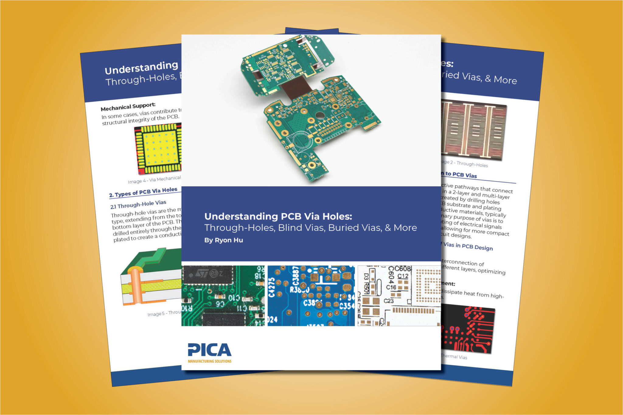
PDFVia design and fabrication guide
Connect every layer reliably
Choose the right via forevery PCB connection.
This engineering guide explains how through-holes, blind vias, buried vias, microvias, and via-in-pad structures support routing density, thermal management, and dependable multilayer connectivity.
- 01Compare essential via types
Understand where through-holes, blind vias, buried vias, microvias, and via-in-pad are used.
- 02Plan the fabrication process
Learn how laser drilling, electroplating, and via filling enable reliable multilayer connections.
- 03Optimize electrical and thermal performance
Apply spacing, signal-integrity, and thermal guidance for HDI, RF, and fine-pitch BGA layouts.
Request the full white paper.
Complete the short form and we’ll send the resource to your inbox.
Loading secure form…
Your information is used only to fulfill your request and provide relevant PICA communications.