


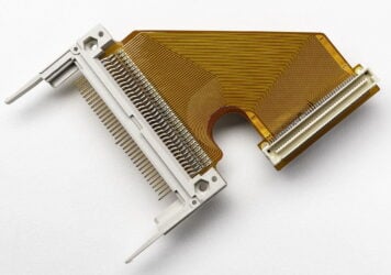
Rigid-Flex PCB vs. Flex PCB with a Rigidizer: Benefits, Differences, Costs, and Best-Fit Applications
When engineers need a circuit that can bend, fit into tight spaces, or replace bulky wire harnesses,...

PCB, Flex & PCBA Cost Pressures in 2026: What OEMs Need to Watch
Electronics manufacturing is heading into 2026 under pressure from several directions at once. Rising metals costs, laminate and prepreg repricing,...
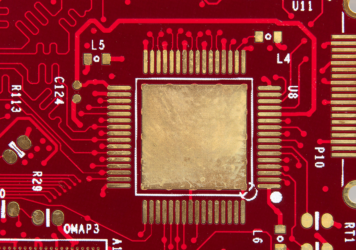
How Flex PCBs Are Shielded for EMI and RFI Protection
Electromagnetic interference (EMI) and radio frequency interference (RFI) can disrupt signal quality, create data errors, and reduce...
How to Choose Flex PCB Materials for Bend Reliability, Heat, and Cost
A practical step-by-step method for choosing materials that hold up in bending, assembly, and real environmentsFlex material...
Metal Core PCBs (MCPCBs): Thermal Muscle for High-Power Electronics
Modern electronics pack more power into tighter spaces than ever. That heat has to go somewhere.
Designing for HDI PCB and Fine-Line Etching: What You Need to Know
As devices shrink and performance demands grow, engineers are turning to High-Density Interconnect (HDI) technology to pack...
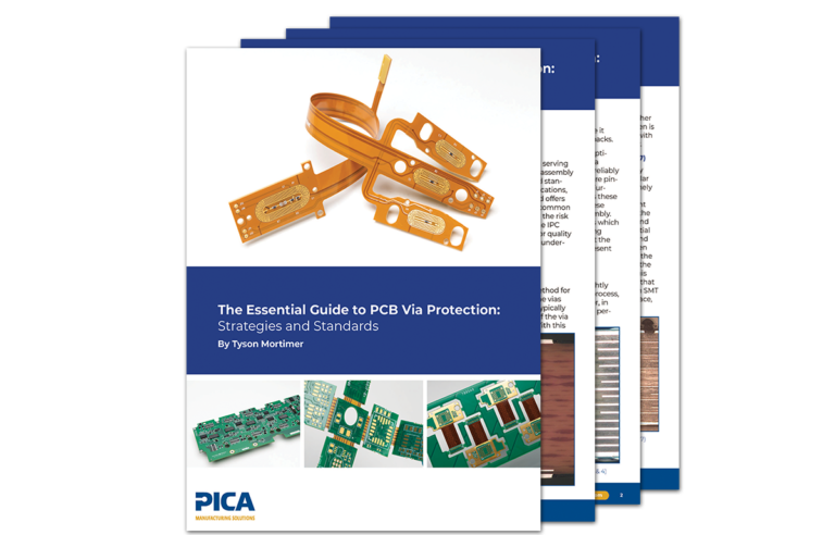
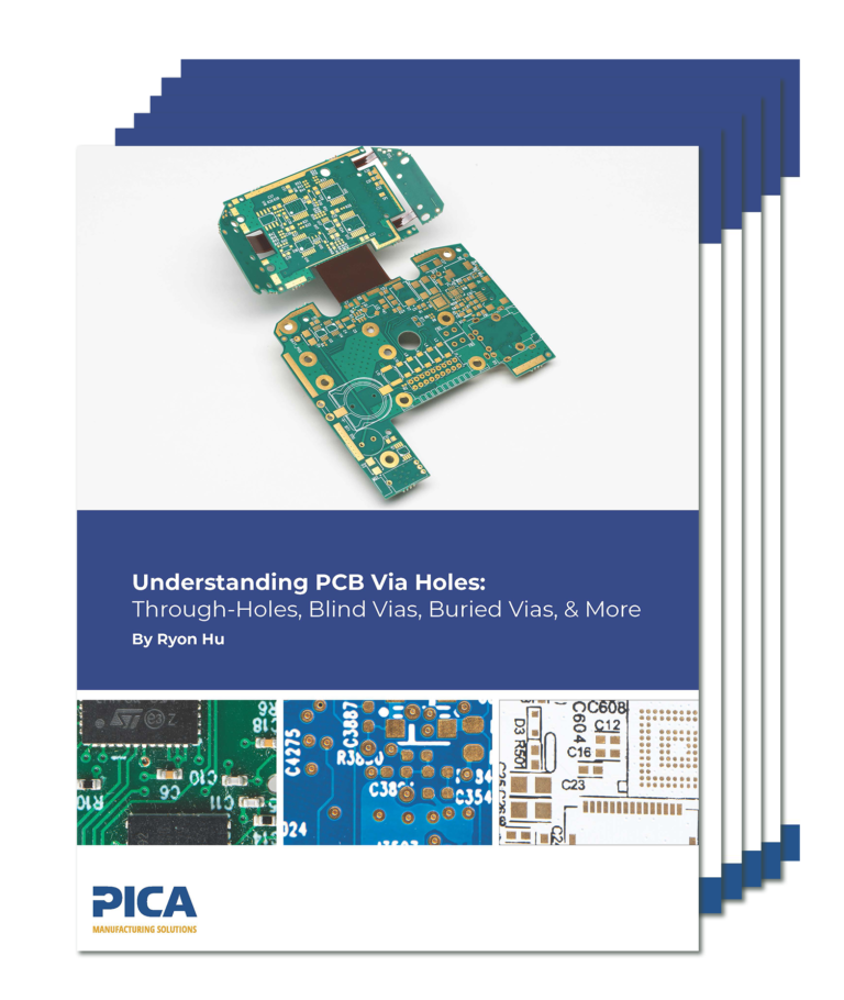
Understanding PCB Via Holes: Through-Holes, Blind Vias, Buried Vias, & More
Printed Circuit Boards (PCBs) form the backbone of modern electronic devices, providing the physical platform for mounting and interconnecting...
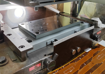
Understanding Tooling in Flexible Printed Circuit Manufacturing: Mechanical Tooling (Part 1)
At PICA Manufacturing Solutions, producing high-quality Flexible Printed Circuits (FPCs) involves a variety of specialized tooling and processes. This blog...