IC Substrate & Carrier Solutions
High-Density Chip-Carrier Architectures for Advanced Packaging
IC substrate carriers bridge the gap between bare die and printed-circuit board, delivering ultra-fine routing, high-reliability materials and precision micro-via architectures. At PICA, we provide IC-substrate carriers designed for compact packaging, thermal stress mitigation and high-frequency interconnects.
Learn more about flex PCB substrates. Read more here.
Why Choose IC Substrate & Carrier Solutions?
• Ultra-Fine Conductors – Typical line/space down to 30/30 µm; R&D builds to 20/20 µm.
• Micro-via Precision – Via diameters as small as 50 µm using laser-defined processes.
• Thermal & Dimensional Stability – Materials with Tg in the 250-300 °C range and X/Y CTE as low as 2-5 ppm/°C.
• Advanced Packaging Applications – Ideal for flip-chip modules, SiP, CSP, SLP, and other high-density integration.
• Early DFM & Material Support – PICA partners with design engineers to define stack-ups, material sets and micro-via architectures from concept to production.
IC Substrate & Carrier Capabilities – Highlights
• Supports line/space geometry of 30/30 µm, and R&D down to 20/20 µm.
• Laser-defined via diameters down to 50 µm.
• High-performance materials: BT resin systems, ceramic substrates, high Tg laminates.
• Low CTE (< 5 ppm/°C) substrates and tight dimensional control for high-reliability packaging.
• Specialist support for flip-chip, SiP, and other advanced packaging formats including substrate-like PCBs (SLP).
• Engineering collaboration from stack-up definition through manufacturing and testing for high-density chip platforms.
Global Design & Manufacturing Support
PICA offers full-lifecycle support—from engineering in the U.S. through advanced manufacturing, with deep expertise in micro-via architecture, substrate material selection and high-density layout. Engaging early in the project allows us to align material sets, define high-performance stack-ups, and ensure manufacturable, high-yield substrate carriers for sophisticated packaging applications.
Benefits of IC Substrate & Carrier Solutions
Miniaturization & Density
Carrier substrates let you route massive I/O counts in a small footprint, enabling compact packages, stacked dies and multi-chip modules.
High-Frequency & Signal Integrity
Ultra-fine conductor routing and high-performance materials support demanding signal/power delivery requirements in RF, compute-intensive and high-speed applications.
Thermal & Dimensional Reliability
With high Tg laminates and low CTE substrates, these carriers maintain structural and electrical integrity under thermal cycling and high-stress packaging conditions.
Integration Flexibility
From traditional PCB form-factors to substrate-like PCBs (SLP), flip-chip and SiP modules, carrier solutions let you bridge chip to board with optimized interconnect architecture.
High-Yield Manufacturability
By defining design rules and materials early, PICA helps reduce risk, improve yield, and support production-ready volumes for advanced packaging.
Markets We Serve with IC Substrate & Carrier Solutions
High-Performance Computing & Server Platforms
Large I/O packages, multi-chip modules and dense chip carriers benefit from the miniaturization and routing density of substrate carriers.
Mobile & Consumer Electronics
Premium smartphones, foldables, wearables and IoT devices require ultra-compact, high-density carriers to support advanced features and form-factors.
Automotive & ADAS Systems
Advanced driver assistance systems (ADAS), sensor hubs and compute modules depend on reliable packaging with thermal robustness and high signal integrity.
Networking & Telecommunications
5G/6G modules, optical transceivers and high-speed network cards require dense interconnect substrates with controlled impedance and thermal performance.
Aerospace, Defense & Mission-Critical Systems
When reliability, miniaturization and performance are non-negotiable, substrate carriers deliver the interconnect backbone for rugged, high-density modules.
The blogs featured below expand on this page’s content, offering detailed insights into specific design, manufacturing, and application topics that provide added relevance and deeper context for engineers and decision-makers.
Flex PCB Substrate Materials Beyond Polyimide: PET, PEN, LCP, PTFE, PEI, and PEEK
PET vs PEN, LCP, PTFE/fluoropolymers, and specialty films like PEI/PEEK: when each wins, where each struggles, and what it means...
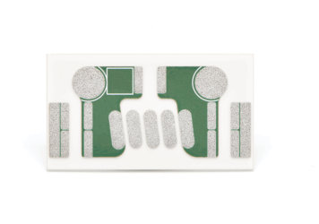
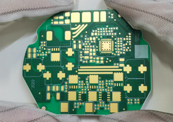
Compact Power, Cooler Systems: The Case for Ceramic PCBs in Modern Electronics
Modern electronics are expected to run hotter, switch faster, and survive harsher environments than ever. Standard FR-4 hits its limits...
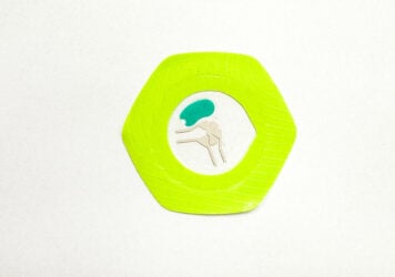
Biocompatible Substrates for Flex and Rigid PCBs
In the expanding world of medical devices, and wearables, the demand for biocompatible substrates...
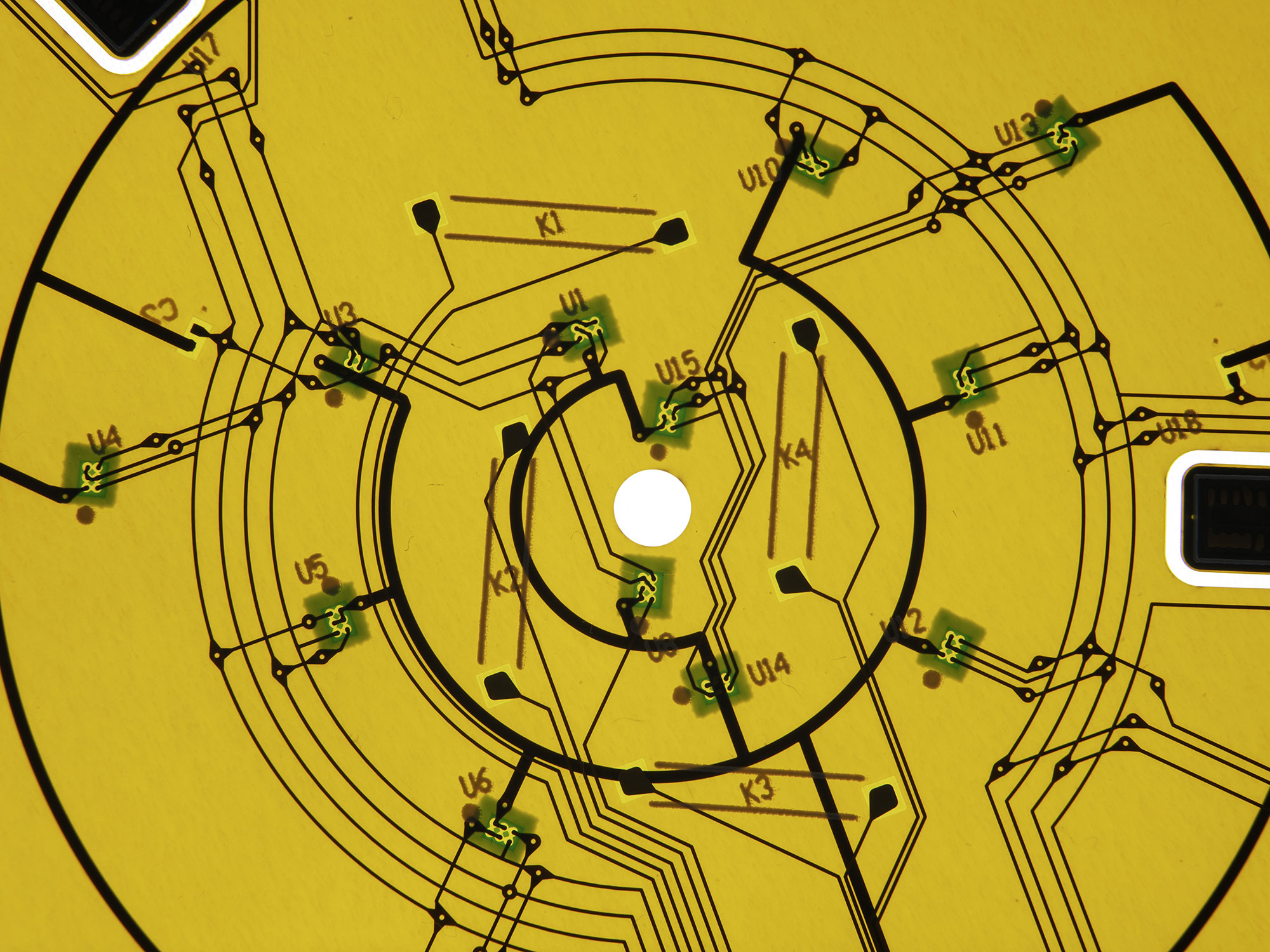
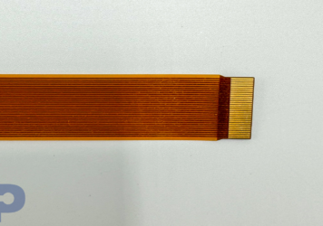
Adhesiveless Technologies for Flexible Circuits: Unlocking Next-Generation Performance
In the world of flexible electronics, the shift from traditional flexible copper-clad laminates (FCCLs) to adhesiveless materials represents a significant...
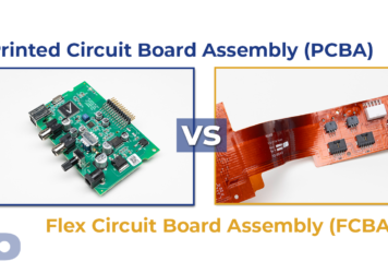
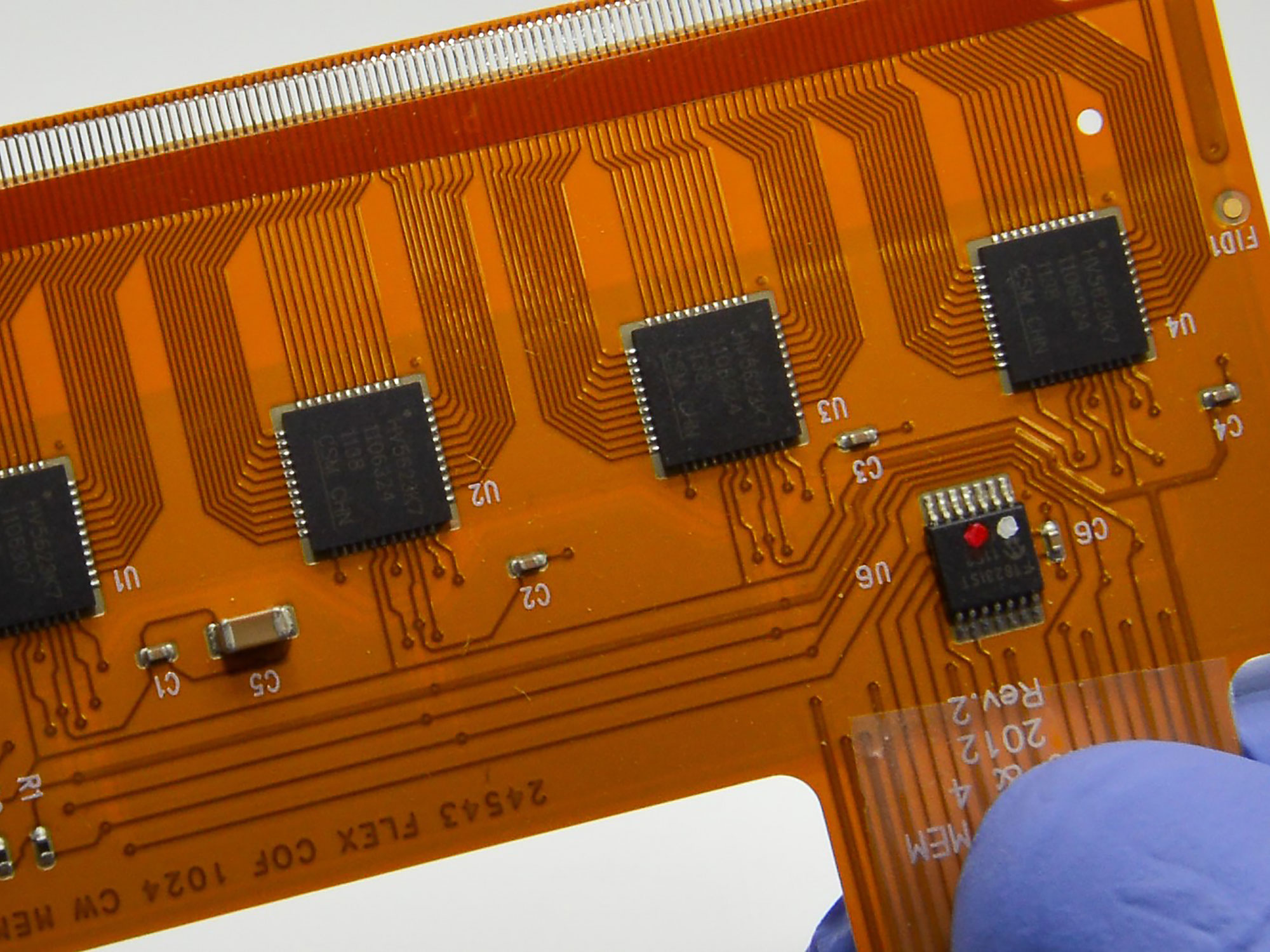
PCBAs vs. FPCAs: Understanding the Differences
PCBAs (Printed Circuit Board Assemblies) and FPCAs (Flexible Printed Circuit Assemblies) are both integral to the...
Enhancing Polyimide Surface Properties for Superior Bonding in Flexible Printed Circuits
The general scope of this article is to discuss methods for treating and characterizing the surface of Kapton, a...
Case Study: Innovating Medical Healthcare Technology with Rigid Flex PCB Design
Customer Overview: The customer in this case study is a leading company in the healthcare technology sector, known for its...
The Rise of Ceramic Substrate Printed Circuit Board
Ceramic substrate PCBs (Printed Circuit Boards) represent a significant advancement in circuit board technology, especially when compared to traditional...


