Guide to PCB & FPC Manufacturing Processes
FlexPros2025-06-25T20:02:55+00:00This blog is an excerpt from the white paper Guide to PCB & FPC Manufacturing Processes: Subtractive, Semi-Additive & Additive Techniques. Request the full white paper here.
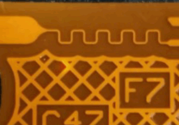
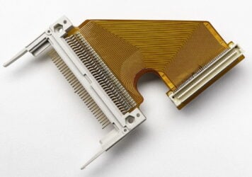
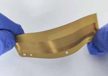
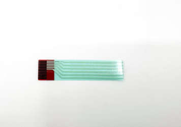
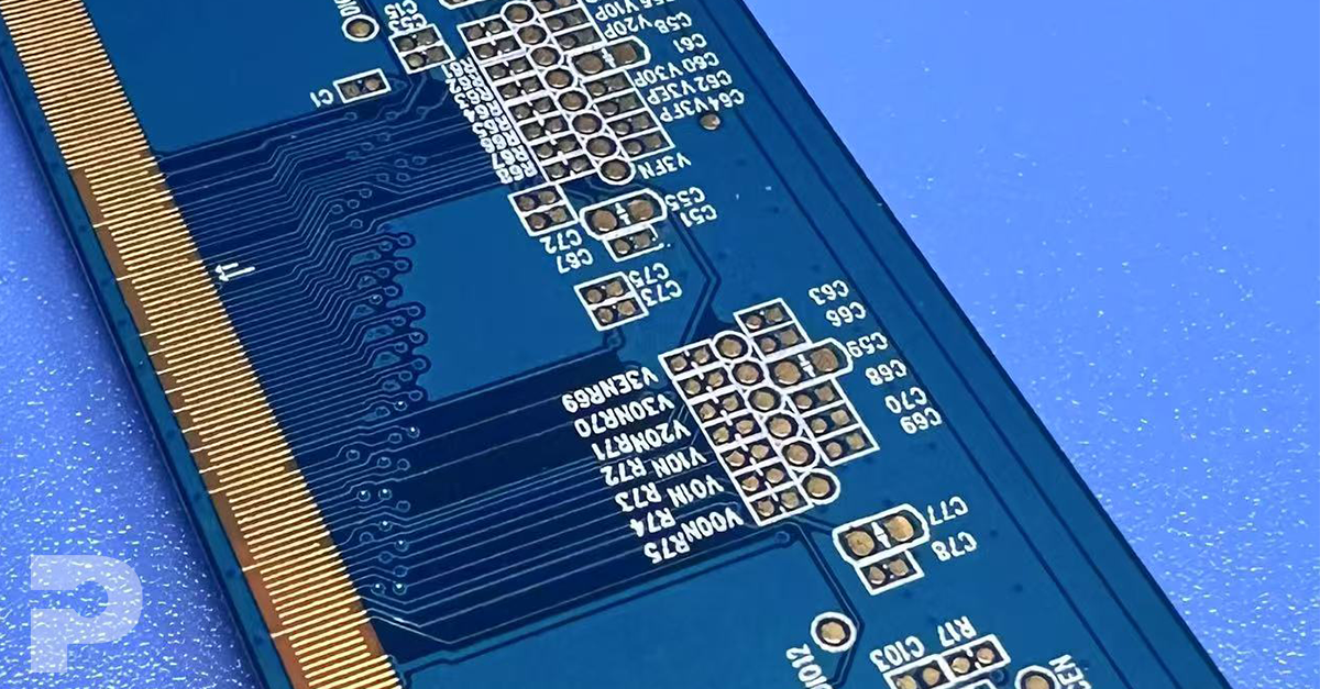
As PCBs and flex circuits evolve to support smaller devices, denser routing, and higher performance, engineers are turning to more advanced copper patterning processes. Whether you’re designing a high-density rigid board, a compact wearable with flex arms, or a hybrid rigid-flex assembly, the way you build copper features matters, especially as line/ space requirements drop below 75 μm.
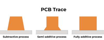
This guide compares three major methods of forming copper features on PCBs and flex circuits:
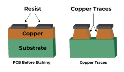
• Subtractive Etching (traditional)
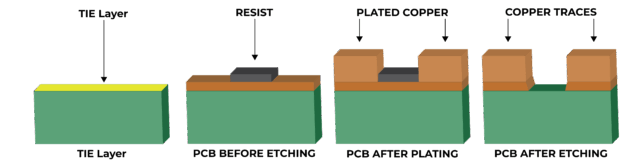
• Semi-Additive Process (SAP / mSAP)
• Fully Additive Process (e.g. inkjet or electroless)
We’ll explore how each method works, where it’s best used, and what designers need to consider when building modern rigid, flex, or rigid-flex designs.

Image 1 – PCB Traces
Subtractive Process: The Traditional Workhorse
What it is?
Subtractive PCB fabrication starts with a copper-clad laminate (typically 0.26 to 2 oz or 9 to 70 μm copper) and removes unwanted copper using chemical etching. This is the most common approach for both rigid boards and single – or double-layer flex circuits.

Image 2 – Subtractive Process
Process Steps
• Start with copper-clad substrate: Use a laminate with copper foil (typically 9–70 μm) already bonded to one or both sides of the dielectric core. For flex, this is often polyimide with rolled annealed copper.
• Apply and expose photoresist: A dry-film or liquid photoresist is laminated or coated onto the copper surface. The board is then exposed to UV light through a phototool, hardening only the areas meant to remain as copper traces.
• Etch away exposed copper: A chemical etchant (e.g. ammoniacal cupric chloride or ferric chloride) removes unprotected copper, leaving only the hardened photoresist-covered pattern behind.
• Strip resist: The remaining photoresist is chemically stripped to reveal the finished copper traces underneath.
• (Optional) Plate vias and apply surface finish: If the board includes plated-through vias, they are electroplated at this stage. Then, a surface finish (such as ENIG, HASL, or OSP) is applied to protect the copper and improve solderability.
Download the full white paper to get the final section on Fully Additive Process: For Printing and Flexible Hybrid Electronics.
• Rigid PCBs, flex circuits, and some rigid flex
• Standard-density consumer, industrial, and automotive designs
• Line/space ≥ 75 μm (3 mil)
Advantages
• Well-established and widely available
• Cost-effective for mid-density designs
• Supports both rigid and flexible substrates
Limitations
• Over-etching creates trapezoidal trace profiles—problematic for impedance control
• Hard to achieve <50 μm features due to side etch
• Creating more copper waste
• In flex circuits, over-etching can weaken trace integrity
Semi-Additive Process (SAP/mSAP): The HDI & Flex Enabler
What is it?
The semi-additive process (SAP) or modified semi-additive process (mSAP) begins with a very thin seed layer of copper (1–5 μm), adds copper where needed using electroplating, and then removes the rest of the seed layer.
It enables much finer features and cleaner profiles, especially important in HDI and flex circuit designs where space and bend radius are limited.

Image 3 – Semi Additive Process
Process Steps
Start with a dielectric core and apply tie layer: A thin adhesion or tie layer (often chromium or similar) is deposited in a vacuum chamber onto the dielectric core to promote adhesion. This is followed by sputtering or depositing a very thin copper seed layer, typically 1–5 μm thick. (EDIT Process Image)
Apply and expose photoresist: A photoresist is laminated, exposed to UV through a photomask, and developed to define the copper trace areas.
Electroplate copper onto desired features: Copper is electroplated only where the photoresist has been cleared, building up traces and pads to the required thickness.
Strip resist: The remaining photoresist is removed, exposing the unplated seed copper layer underneath.
Etch away unplated seed layer: A microetch removes the thin seed copper and tie layer in the background, leaving behind only the plated copper features.
Final finish and via plating: Additional steps like via copper plating, surface finish application (e.g. ENIG, OSP), and soldermask coating follow, depending on design requirements.
Where It’s Used?
• HDI rigid PCBs (smartphones, wearables, medical)
• Multi-layer flex and rigid-flex circuits
• Designs with fine-pitch BGAs or impedance control
• Line/space down to 15–30 μm (0.6–1.2 mil)
Advantages
• Supports fine features and tight component pitch
• Near-vertical trace walls improve impedance accuracy
• Minimizes undercut—critical for flex circuits where mechanical reliability matters
• Less copper waste vs. subtractive
Limitations
• Higher cost and longer processing time
• Requires more advanced imaging and plating control
• Not all PCB/flex vendors can support SAP in volume
This blog is an excerpt from the white paper Guide to PCB & FPC Manufacturing Processes: Subtractive, Semi-Additive & Additive Techniques. Request the full white paper here.
Please contact us here with any PCB & FPC questions.