Designing High Voltage PCBs: Key Layout and Material Considerations
When working with high-voltage circuits, design priorities shift. While many PCBs focus on high-speed signaling, impedance control, or component density, high-voltage designs prioritize safety, insulation, and spacing. Whether you’re developing an industrial power controller, EV subsystem, or medical device, successful high-voltage PCB design demands a clear understanding of creepage, clearance, and material behavior under electrical stress.
At PICA Manufacturing Solutions, we regularly support engineers building PCBs for voltages well above 100V—sometimes reaching into the kilovolt range. Here’s what you need to know to design them right the first time.
What Counts as “High Voltage”?
There’s no single global definition, but most PCB designers start applying high-voltage layout rules around:
• >100V DC
• >30V RMS AC
• >60V continuous between conductive surfaces
In regulated environments (medical, industrial, automotive), even 48V systems may require special treatment due to safety standards and compliance.
Key Terms Engineers Must Understand
1. Clearance
The shortest distance through air between two conductive features.
• Affects arcing risk and air ionization breakdown.
• Influenced by humidity, altitude, and environmental contaminants.

2. Creepage
The shortest path along the surface of the PCB substrate between conductors.
• Especially critical for long-term reliability in humid or dirty environments.
• Surface contaminants and tracking can compromise insulation.

3. Working Voltage
The continuous operating voltage expected between two conductors—not the transient or peak voltage.
• Used to determine clearance and creepage requirements per IPC or IEC standards.
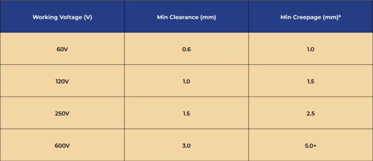
Recommended Spacing Guidelines
Key Design Practices for High Voltage PCBs
1. Widen Trace Spacing
Even if your signals operate at low current, spacing matters when voltage increases.
• Refer to IPC-2221B or UL 796 for specific clearance rules.
• Increase spacing in areas prone to condensation, humidity, or airborne debris.
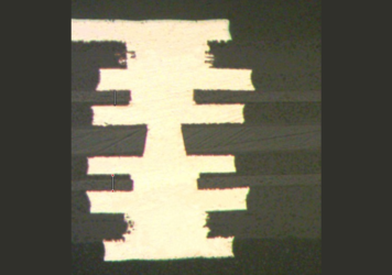
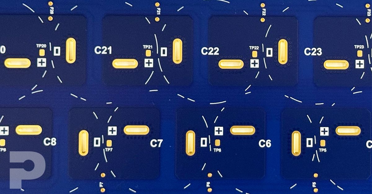
2. Use Slots or Cutouts to Improve Creepage
Non-plated isolation slots or grooves between conductors can increase surface path length.
• Often used in power supplies, relays, and safety barriers.
• Ensure slots are wide enough to maintain creepage even after solder mask application or board cleaning.
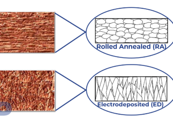
3. Choose Materials with High CTI Ratings
CTI (Comparative Tracking Index) measures a material’s resistance to surface tracking.
• CTI ≥ 600V is preferred for high-voltage designs.
• Standard FR-4 is typically rated between 175V and 300V.
• Ask your fabricator for available high-CTI laminate options if needed for compliance.
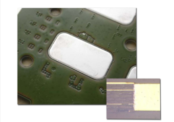
4. Add Conformal Coating for Extra Protection
Conformal coating helps seal the board surface, increasing effective creepage distance and protecting against moisture and dust.
• Common coatings include acrylic, urethane, or silicone-based materials.
• Especially useful in industrial, automotive, or outdoor applications.

5. Smooth Out Corners and Avoid Copper “Points”
Sharp copper angles can concentrate electric fields and promote corona discharge or dielectric breakdown.
• Use rounded corners on high-voltage traces.
• Avoid unconnected via stubs or narrow copper slivers near high-voltage nets.
Thermal and Mechanical Considerations
Heat can also degrade insulation performance over time.
• Separate heat-generating components from sensitive high-voltage zones.
• Use thermal reliefs, heatsinks, or copper pours to manage localized temperature spikes.
• Select laminates with high thermal stability for demanding environments.

Final Thoughts
Designing high-voltage PCBs isn’t just about spacing—it’s about making smart decisions around layout, materials, environmental exposure, and long-term safety. Even small oversights in creepage or insulation can result in early failure, arcing, or compliance issues.
At PICA Manufacturing Solutions, we help customers design safe, reliable, and compliant PCBs for a range of high-voltage applications. Whether you’re building industrial controls, automotive systems, or critical infrastructure electronics, our engineering team can support you from early layout through to final fabrication.