
| Product Process | Project | Process Capability | ||||
|---|---|---|---|---|---|---|
| Laminate Shear |
Board Thickness | 0.4-0.8mm | 1.0-1.6mm | 1.7-2.0mm | 2.1-4.0mm | |
| Board Tolerance | ±0.05mm | ±0.075mm | ±0.10mm | ±0.12mm | ||
| Panel Size |
|
Aluminum array | Max length is 1.2m, but when length >600mm, width size must be <333mm |
|||
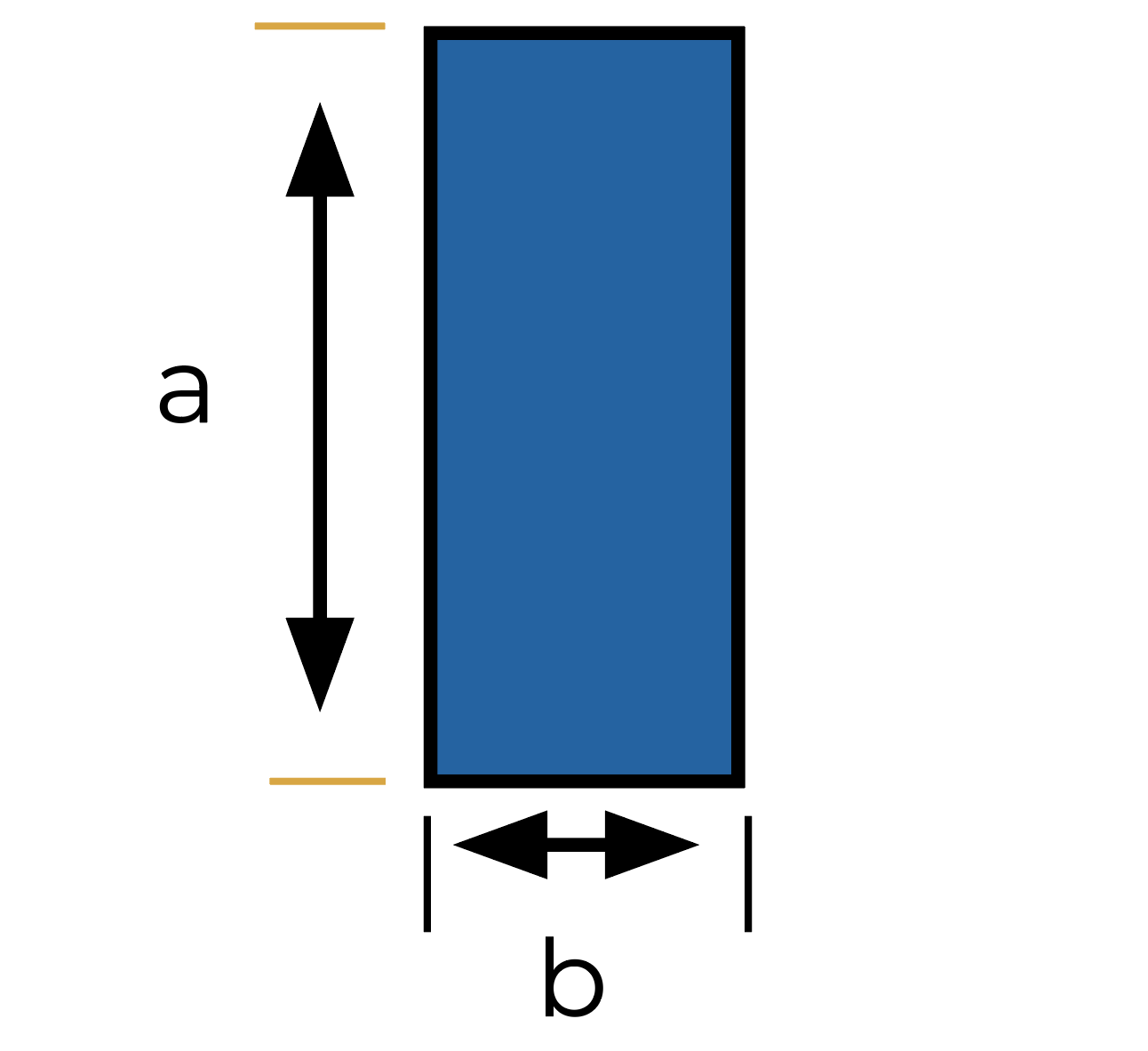
| AL plate panel | a≥500mm, b≤300mm | |||||
| Copper substrate panel | Copper substrate panel size 500x600mm Max Thermoelectric separation of copper substrate panel size 300x350mm Max |
|||||
| Working panel size |
|
CNC Routing | 7.5mm≥a and b≥5mm | |||
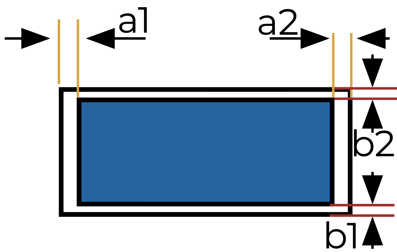
| V-cut | 11mm≥a and b≥5mm a1+a2≤18mm, b1+b2≤18mm |
|||||
| Laminate Shear Tolerance | +/-1mm | |||||
| Drill | Drill position tolerance | ≥0.05mm | ||||
| Hole to Hole | ≥0.1mm | |||||
| Hole Size Tolerance | Single Fr4 | ±0.05mm | ||||
| Single AI | ±0.05mm | |||||
| Double-sided AI and Copper substrate board | PTH/1 oz/2 oz | ±0.05mm | ||||
| NPTH | ±0.05mm | |||||
