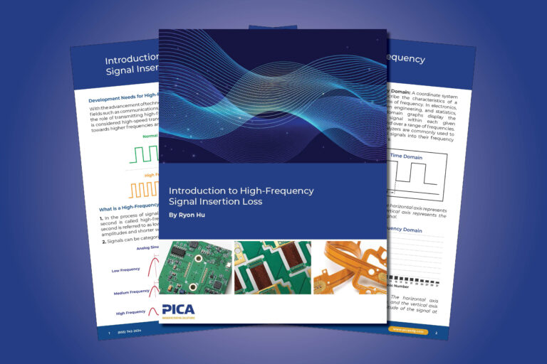
Download Introduction to High Frequency Signal Insertion Loss by Ryon Hu.
Introduction to High Frequency Signal Insertion Loss
Explore the fundamentals of high-frequency signal insertion loss in PCB design with this technical overview from PICA Manufacturing Solutions. As signal frequencies exceed 50 MHz in advanced telecom, automotive, and networking applications, minimizing insertion loss is critical for maintaining signal integrity and performance. This guide explains the core causes of insertion loss—dielectric loss (Dk/Df) and conductor loss due to surface roughness and skin effect—and outlines how advanced materials like low-Dk/Df laminates and RTF, VLP, or HVLP copper foils can dramatically reduce signal degradation. Learn how Fourier transforms, time vs. frequency domain analysis, and industry-standard Delta-L testing are used to evaluate high-speed transmission performance across PCBs.

