Printed Circuit Board (PCB) Via Protection: Strategies and Standards
Tyson Mortimer2026-03-13T15:09:34+00:00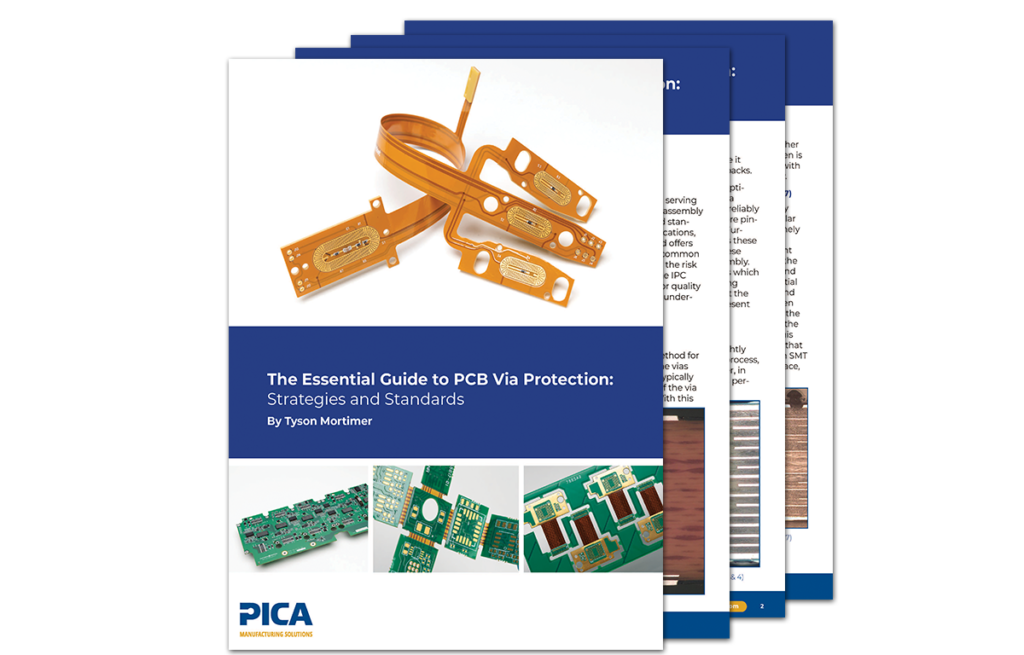
This blog is an introduction to a larger white paper that features 7 different via protection types. Download the full white paper to continue reading The Essential Guide to PCB Via Protection: Strategies and Standards. In the full white paper you’ll learn about Filled Via Cap Plating, Coverlay Tented Via, and Copper Filled Micro-via. Click the button below to request the full white paper.
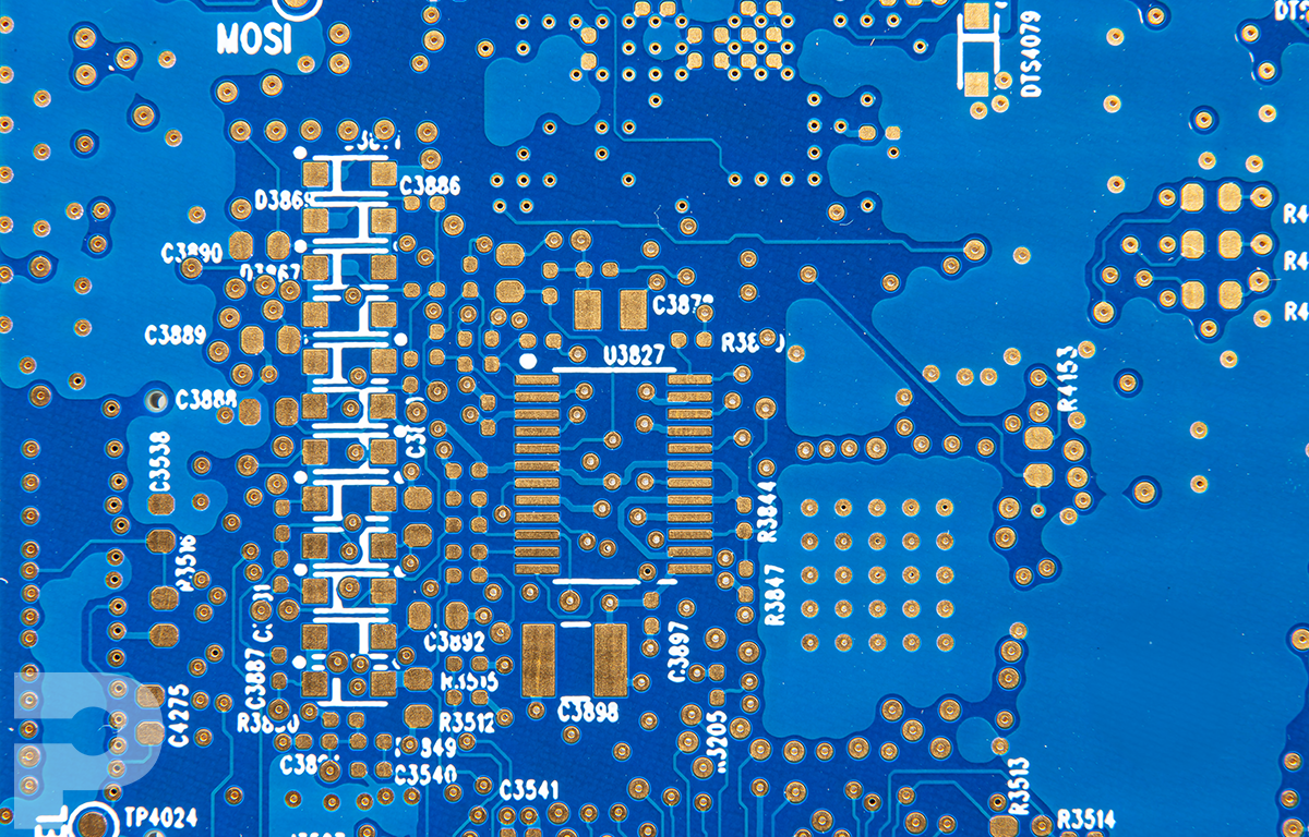
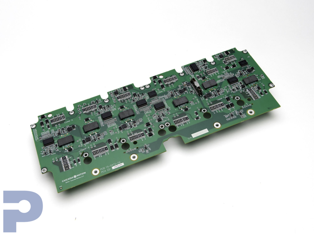
All too often Printed Circuit boards are viewed as simple two-dimensional surfaces. Nowhere is this oversimplification more evident than in the complex structure of Vias. These essential structures are critical to the form and function of any PCB with more than a single layer. Without these vias modern electronics would not be possible in the way we know them today. This paper delves into the importance of via protection, what the Institute for Printed Circuits (IPC) recommends, the types of via protection, their applications, and the inherent limitations and trade-offs.
Why Via Protection is Important
The integrity of vias plays a crucial role in the overall performance and reliability of the final product. PCB vias serve as the electrical connections that pass through the layers of a PCB, acting as conduits for signals and power between different layers. These tiny, yet essential, components are vulnerable to various issues such as solder flow, environmental exposure, mechanical stress. This makes via protection a critical yet often overlooked aspect of a PCB design.
What IPC Has to Say About Via
Protection
The IPC, a global trade association serving the printed board and electronics assembly industries, provides guidelines and standards for via protection in its publications, notably the IPC-4761. This standard offers a more in depth look at the most common types of protection used as well as the risk and compromises of each type. The IPC standards serve as a benchmark for quality and thus its definitions are widely understood in the industry.
Maximize your device’s potential with high-quality printed circuit boards! From single-sided to multi-layer designs, we offer advanced PCB solutions tailored to your needs. Explore our capabilities today and connect with our experts to bring your projects to life!
Types of Via Protection:
Unprotected Via
Ironically, an easy and effective method for protecting vias is simply leaving the vias open. This allows the final finish (typically solder or Gold) to coat the inside of the via and keep the copper protected. With this approach there is less risk of entrapped contaminants from the fabrication or assembly process and has no effect on cost.
This approach does have its drawbacks, however. Small holes (<0.014”) may not fully take the surface finish or could even be partially plugged with residual soldermask due to their small size. This limits the types of products which can use this technique to low to medium density PCBs. It also leaves additional exposed metal on the surface, which can be problematic depending on the application.
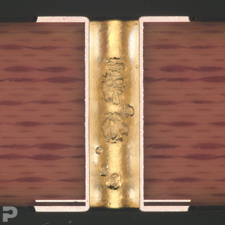
Image 1 – Unprotected Via
Mask Tented Via
A mask tented via is covered with Liquid Photo-imageable (LPI) Mask during the primary coating process and hardened in place during the UV imaging process. This method is also common and free from additional cost. While it eliminates the issue of exposed conductors on the surface it comes with several significant drawbacks. The coating process for LPI mask is optimized for surface coverage, not for via protection. The liquid mask will only reliably cover smaller vias (0.012” or less) before pinholes in the tent become common. Furthermore, the mask only partially fills these vias leaving behind voids. At best, these voids harmlessly outgas during assembly. At worst, they can trap contaminants which can erupt onto the PCB surface during assembly or become trapped against the unprotected copper via walls and present long term reliability issues.
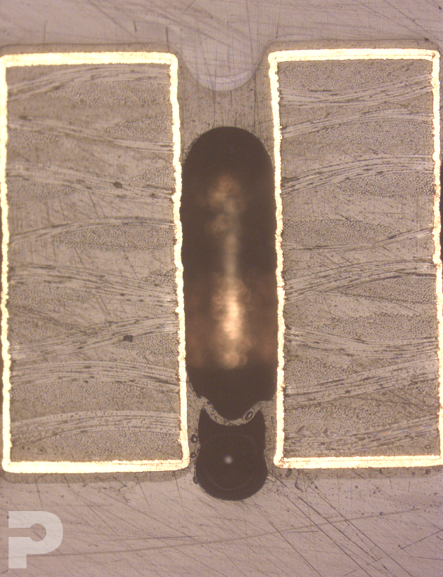
Image 2 – Mask Tented Via
Mask Plugged Via (4761 type 3 & 4)
Plugged vias can be approached slightly differently depending on fabricator process, equipment, and capabilities. However, in general, an additional process step is performed in which LPI mask or specialized Epoxy is forced into the vias. This process is optimized to push the material into the hole with minimal voiding and allows a protected surface as well as a more tightly sealed via.
While this technique is an improvement over a standard mask tented via the process is not without drawbacks. The filling is typically incomplete, leaving one or both sides with dimple or pinhole. While voiding is greatly minimized it is still possible. However, the cost increase for this process is small, making for a good value.
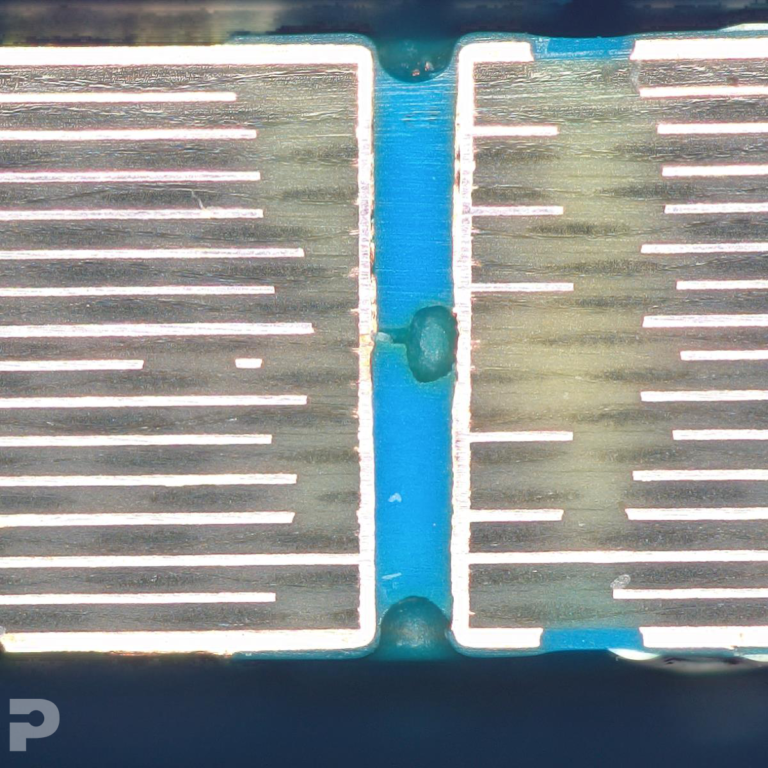
Image 3 – Mask Plugged Via (4761 type 3 & 4)
Epoxy Filled Via (4761 type 5 & 6)
Epoxy filled vias are filled with a low shrinkage non-conductive epoxy resin using specialized equipment. This provides a level and void-free fill resulting in excellent protection across all environments and applications. The low shrink epoxy more closely matches the Thermal Expansion rate of the copper than does LPI, thus improving mechanical support to the vulnerable copper vias during thermal stress. This method is ideal for vias in high-density areas where mechanical strength and air-tight seals are needed.
This array of benefits comes with a higher cost than the previous options and often is only available for either buried vias or with copper cap plating as described next.
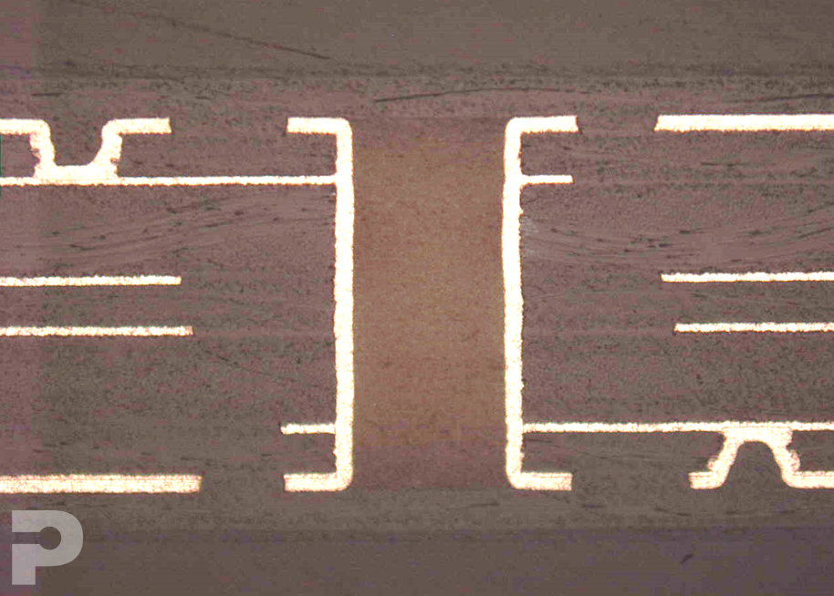
Image 4 – Epoxy Filled Via (4761 type 5 & 6)
Conclusion
Selecting the right via protection strategy depends on many factors and can present a complex choice to designers. Environment, Assembly requirements, design restrictions, product life cycle, application and cost are all important factors. By understanding the different types of via protection and their associated trade-offs, designers and manufacturers can make informed decisions to ensure the reliability and longevity of their PCBs. Whenever possible, have a candid discussion with your manufacturing partner about your design requirements as well as their capabilities.
Download the full white paper to continue reading The Essential Guide to PCB Via Protection: Strategies and Standards. In the full white paper you’ll learn about Filled Via Cap Plating, Coverlay Tented Via, and Copper Filled Micro-via.
Click the button below to request the full white paper.
