Advanced Flexible Printed Circuit Solder Coating Process
Simon Lim2025-08-26T15:44:16+00:00Customer: A leading innovator in inkjet technology, our customer is renowned for their advanced and precise printheads. Serving various sectors within the industrial, commercial, and consumer printing industries, their commitment to continuous innovation and quality underscores their prominent role in the printing technology sector.
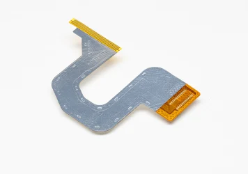
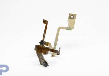
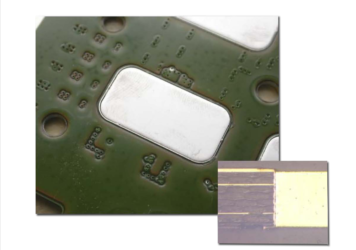
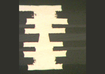
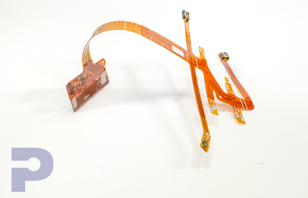
Challenge: The customer required a Flexible Printed Circuit (FPC) with a solder thickness ranging from 12.5 to 37.5um, using SAC 305 solder type, specifically tailored for ACF bonding in their final assembly. The solder was to be applied to a double bare finger of 3.3mm length with 2oz Cu and an ENIG surface finish (Ni: 2.5-3.8um & Au: 0.051-0.153um). This presented a significant challenge as the required thickness was unconventional—either too thick for standard electrolytic plating or too thin and narrow for HASL. Consequently, we tasked our R&D Process Engineering team to develop a customized process that would meet the customer’s specifications. Thanks to my team of talented process engineers, I was able to develop a robust process successfully.
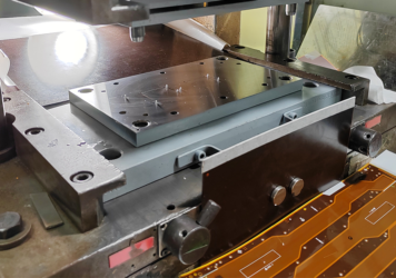
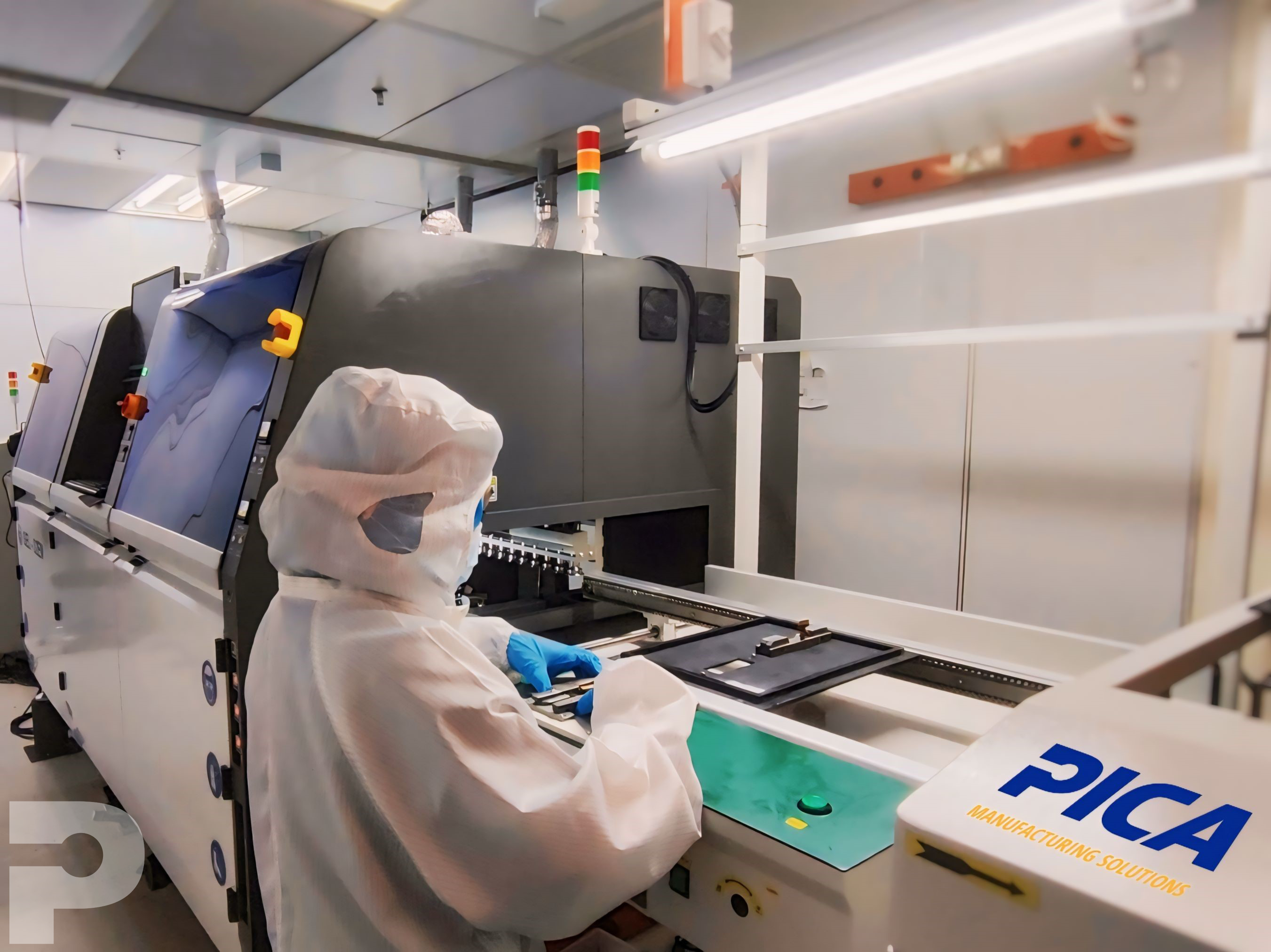
Solution: We initially conducted several evaluations to map out the process, selecting and testing multiple potential methods. We discovered that manual DIP soldering could achieve the desired coating range. However, the main challenge with this method was its inconsistency. Although the coating thickness measurements generally fell within the normal distribution curve, they did not meet the Cpk of 1.33 (3 sigma), often skewing towards the higher end of the spectrum. To address this, we introduced an enhanced process step to remove excess solder, thereby bringing the upper control limit and over-spec coating thickness back to the normal range. Despite the initial success of this customized semi-automatic DIP soldering process, increasing demands for quality control at the ACF assembly stage led us, after ten years, to develop a fully automated solder coating process. Through our exploration, we identified nozzle-selective soldering as the most cost-effective option, considering initial capital expenditures, operational, and maintenance costs. We experimented with:
- Testing three different nozzle types in the existing manual dipping process.
- Using rotating table equipment from Vendor A.
- Employing a semi-automatic vertical solder dip with vibrations from Vendor B.
- Implementing a horizontal wave soldering from Vendor C.
Ultimately, PICA chose the fourth option from Vendor C. Key factors impacting the selective soldering process include solder alloy selection, flux application, preheating parameters, and soldering temperature profiles. In our case, customizing these parameters was crucial to ensure the solder coating fell within the desired range with good Cpk.
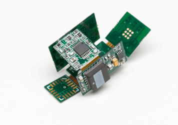
Ready to take your designs to the next level with flexible circuit boards? Explore our high-performance flex PCBs that offer unmatched durability and compact solutions for your most demanding applications.
Result: At PICA, we pride ourselves on listening to our customer’s unique design requirements and developing practical solutions that transition from concept to mass production. Our approach to customizing the selective soldering process allowed us to meet the specific needs of this project, emphasizing the importance of tailored solutions in electronics manufacturing. With over 30 years of design and manufacturing experience, PICA is well-equipped to assist our customers effectively, demonstrating our capacity to handle the complexities of modern electronics assembly where design for manufacturability (DFM) considerations often require compromises to achieve economic viability.
Contact us for any information on Advanced Flexible Printed Solder Coating Process.