


Membrane Switch: Custom Keypads for Reliable User Interfaces
Introduction
When you press the buttons on a medical device, industrial controller, or appliance, there...
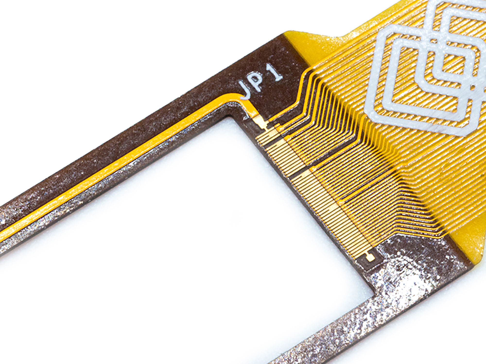
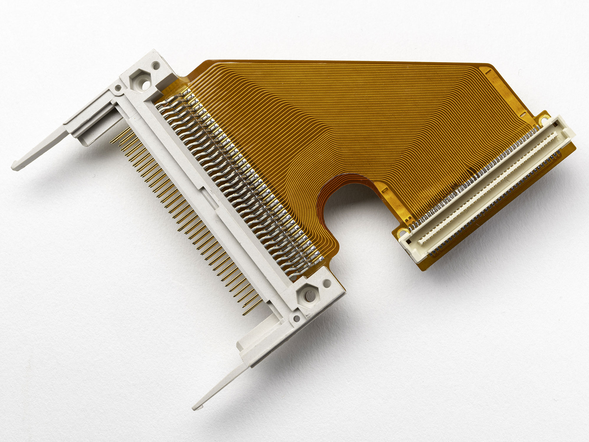
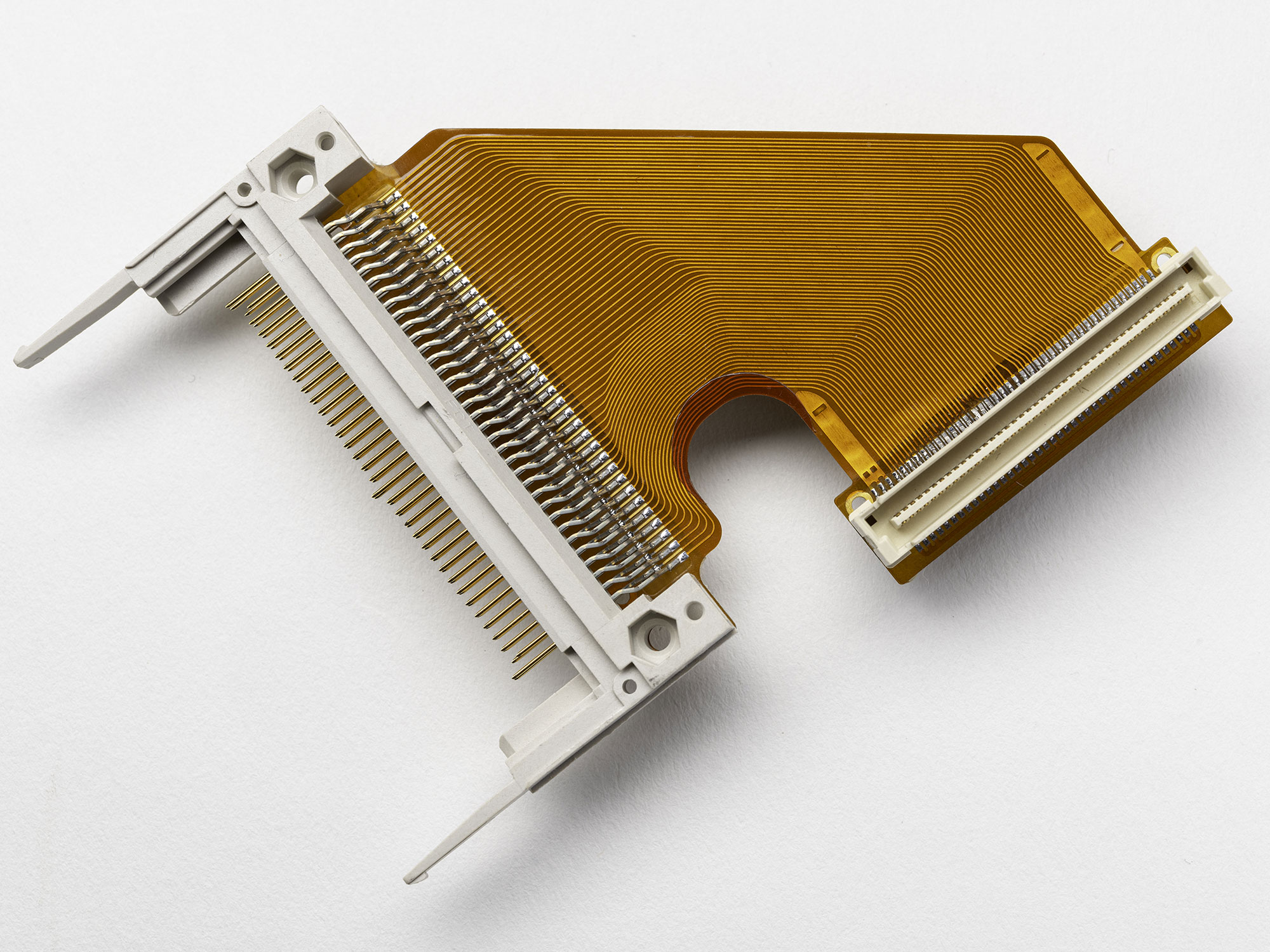
What Is Dynamic Flex PCB? Designing Flexible Circuits for Continuous Motion
Dynamic flex PCBs are where flexible circuit design stops being “just about fitting in tight spaces” and...

SATELLITE 2026: Featured Innovators Driving the Future of Space and Connectivity
SATELLITE 2026 brought the global satellite, space, defense, and communications industries to Washington, D.C....

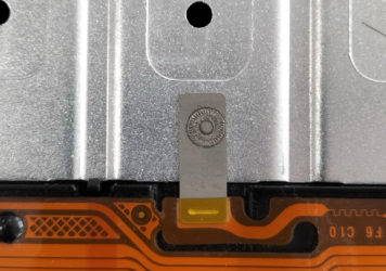
Hole Riveting in Electronics: Reinforcing Connections in Circuit Assemblies
As electronic assemblies become more compact and mechanically complex, manufacturers must ensure that electrical connections remain secure under vibration, handling,...

PCB, Flex & PCBA Cost Pressures in 2026: What OEMs Need to Watch
Electronics manufacturing is heading into 2026 under pressure from several directions at once. Rising metals costs, laminate and prepreg repricing,...

Integrated Flex Circuits and Injection Molding for Electronic Devices
At PICA Manufacturing Solutions, we believe the future of electronics is not built component by component, it is engineered as...
How Flex PCBs Are Shielded for EMI and RFI Protection
Electromagnetic interference (EMI) and radio frequency interference (RFI) can disrupt signal quality, create data errors, and reduce...
Nickel Tab Mounting on Flex Circuits: Strengthening Electrical and Mechanical Connections
Flexible circuits are often chosen for their ability to route signals through tight spaces while tolerating bending...