Fineline Flex PCB Capabilities

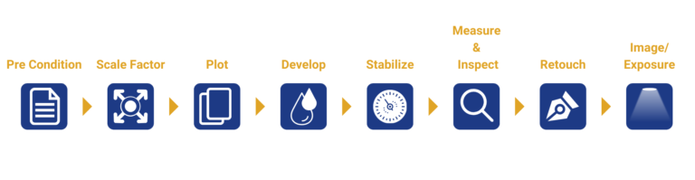
At PICA, we offer advanced design of Fineline Flex Printed Circuit Board (PCB) using state-of-the-art technology. Below are our capabilities in Technology – Laser Direct Imaging and LDI Advantages. For more information on Line Width & Spacing, and PICA LDI Process Capabilities, please fill out the form below to request the full PDF capabilities download or click the button to contact a PICA engineer.

Technology - Laser Direct Imaging

LDI systems “imprint” the printed circuit board (PCB) pattern directly on blank panels, without the use of a photo tool, thus bypassing the image-related stages associated with traditional contact printing, while providing an superior imaging method.

LDI Advantages

  • Fine Line Spacing Capability
  • Improve dimensional stability, and high positional accuracy of the circuit platform
  • Improve Production Yield
  • Short Production Cycle

Traditional Process

LDI Process

Line Width & Spacing Capabilities

Cu Thickness Minimum Line & Spacing After CAD Compensation
1/3oz 1.5mil
1/2oz 2mil
1oz 2.5mil
2oz 5mil

LDI Process Capabilities

Exposure Wavelength Laser (355nm)
Usage Inner/Outer
The method of contraposition UV-marker & CCD
Throughput 200 Hits/HR
Substrate Size max: 609*812mm (24"x32")
Substrate Thickness 0.025 - 5mm (0.001" - 0.2")
Minimum Line & Spacing 38μm (1.5mil) @ 1/3oz. Cu*
Positioning Accuracy (FTG) 12μm (0.45mil)
Side to Side Registration 24μm (0.95mil)
Resolution 6.5μm (0.25mil)

Fill out the form below to request the full Fineline Flex (PCB) capabilities sheet.