


PCB, Flex & PCBA Cost Pressures in 2026: What OEMs Need to Watch
Electronics manufacturing is heading into 2026 under pressure from several directions at once. Rising metals costs, laminate and prepreg repricing,...

Integrated Flex Circuits and Injection Molding for Electronic Devices
At PICA Manufacturing Solutions, we believe the future of electronics is not built component by component, it is engineered as...
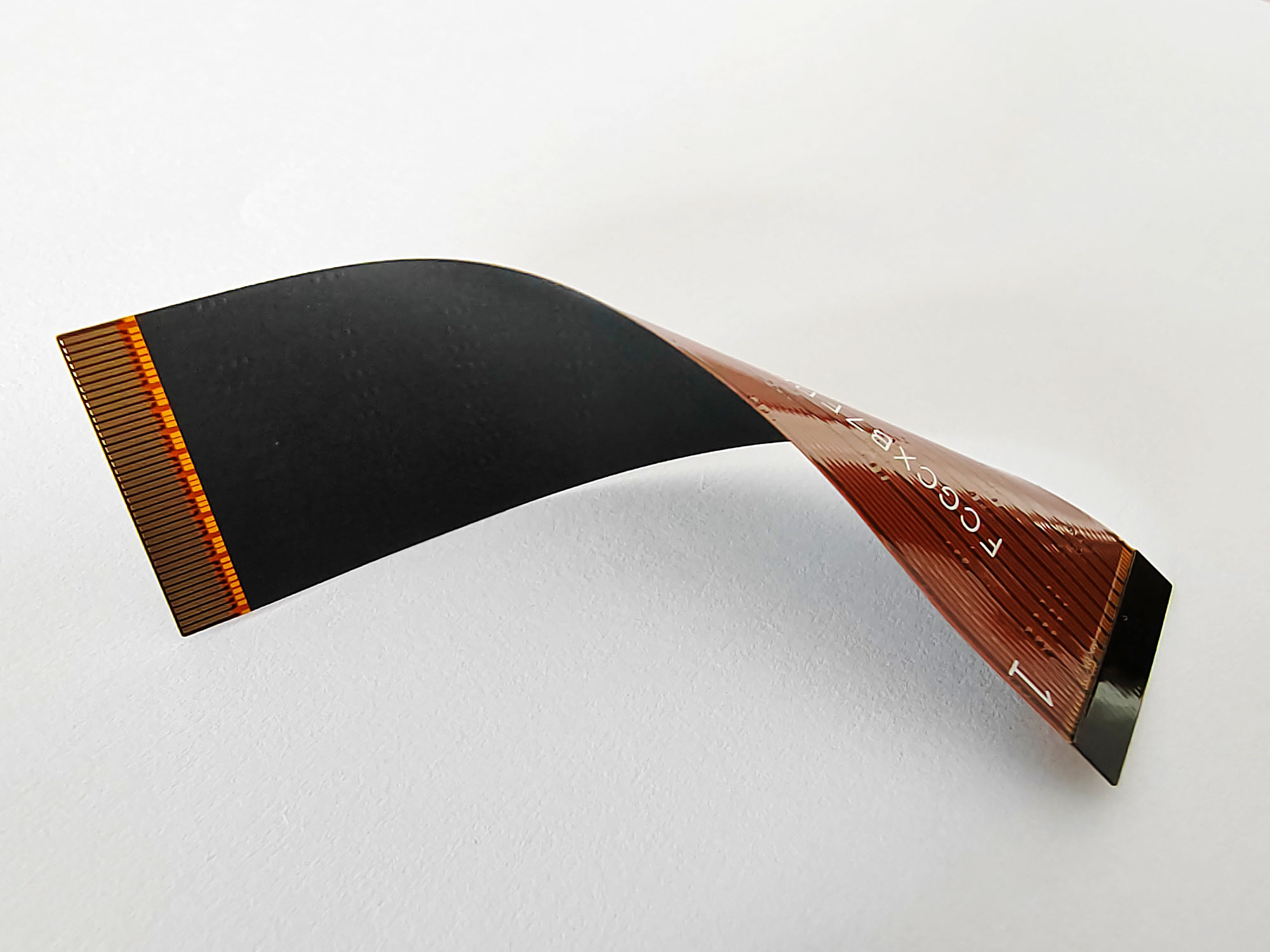
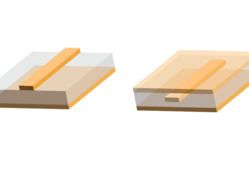
How Flex PCBs Are Shielded for EMI and RFI Protection
Electromagnetic interference (EMI) and radio frequency interference (RFI) can disrupt signal quality, create data errors, and reduce...

Designing PCBs for Medical Devices: Key Considerations & Compliance Tips
PCB design for medical electronics demands more than just electrical functionality. Devices must meet...

Rigid-Flex: The Winning Technology Behind Smart Impact Monitoring Mouthguards
When it comes to sports safety, precision and reliability are non-negotiable. Impact monitoring mouthguards, like those used to measure head...

Biocompatible Substrates for Flex and Rigid PCBs
In the expanding world of medical devices, and wearables, the demand for biocompatible substrates...
Designing for Precision: Controlled Impedance in Flexible Circuits
As electronic devices shrink and signal speeds increase, one design requirement becomes mission-critical: controlled impedance. This is...
Controlled Impedance in Printed Circuit Board Design
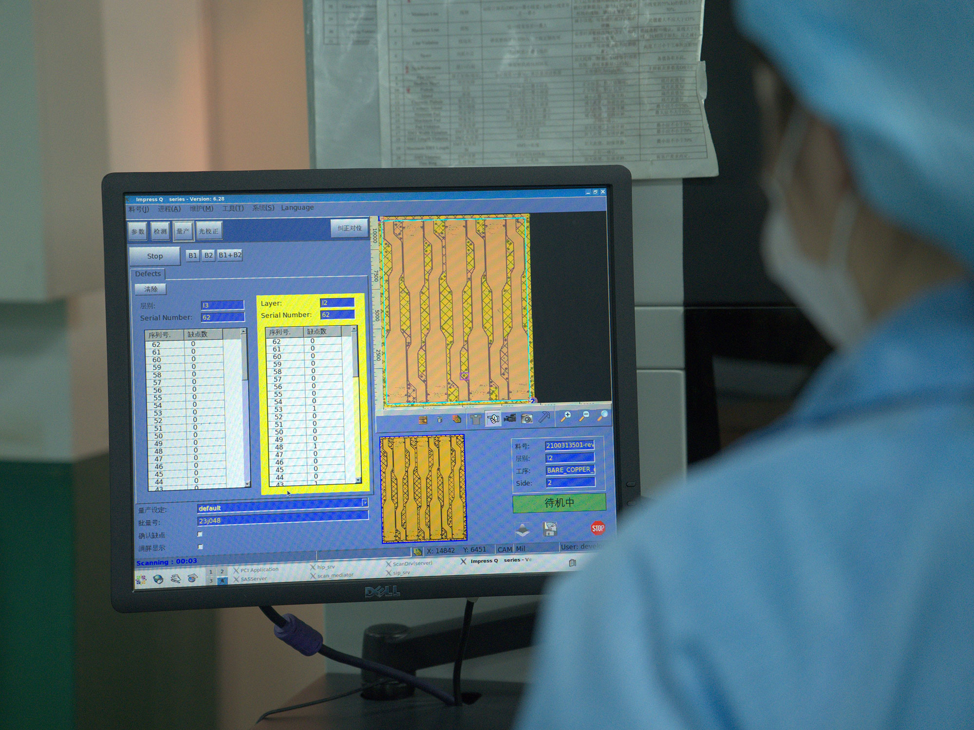
In the design of printed circuit boards (PCBs), controlling impedance is a crucial factor for ensuring optimal signal integrity,...