
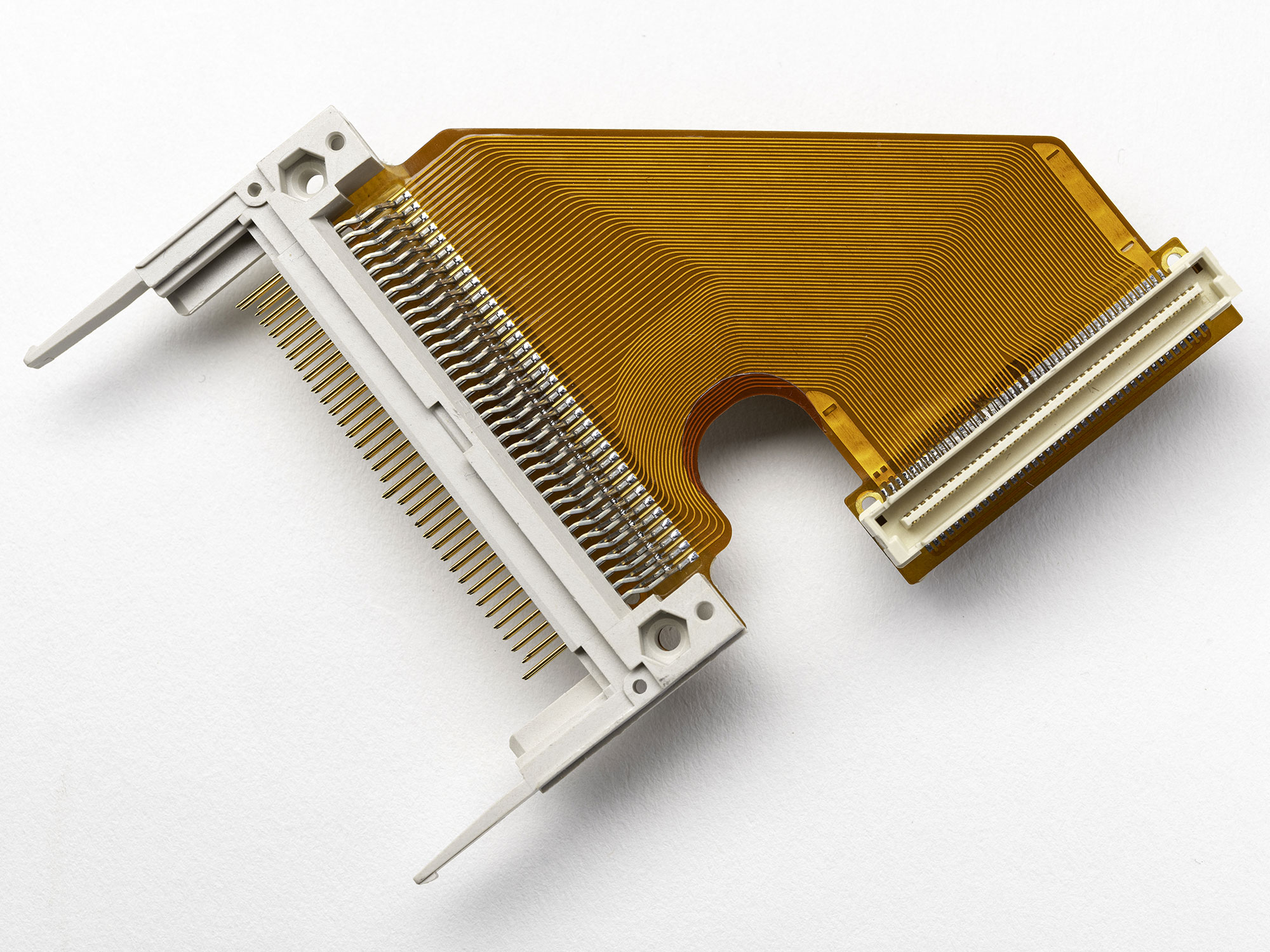
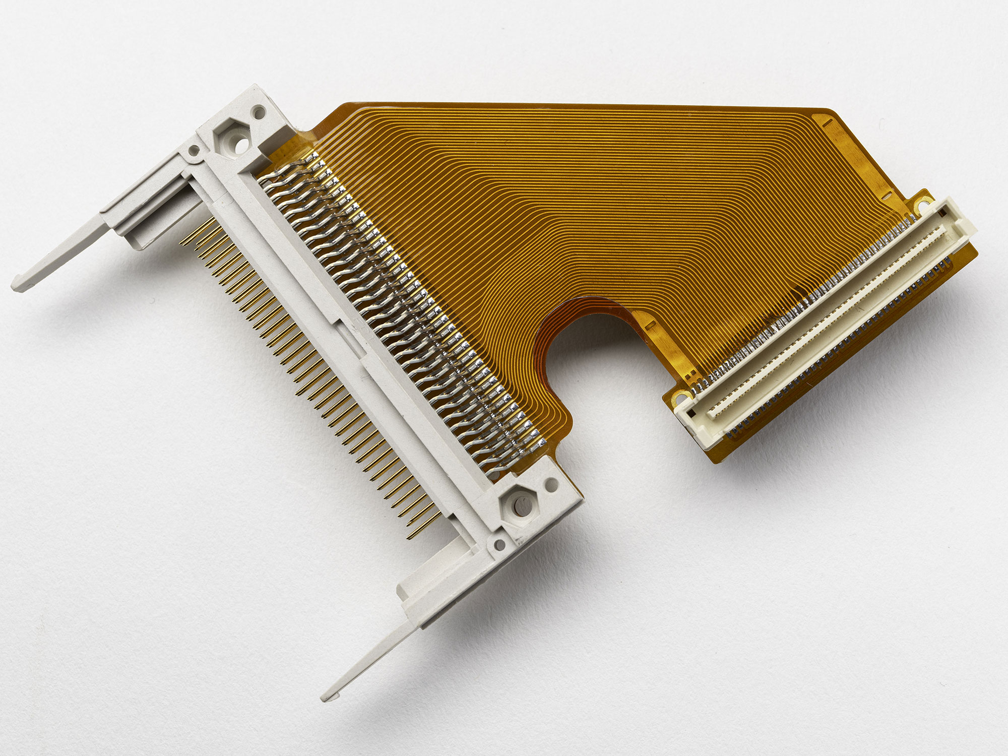


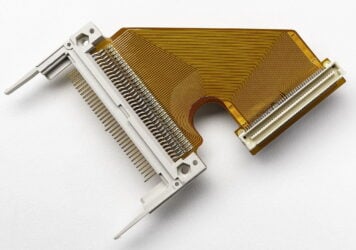
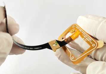
Rigid-Flex PCB vs. Flex PCB with a Rigidizer: Benefits, Differences, Costs, and Best-Fit Applications
When engineers need a circuit that can bend, fit into tight spaces, or replace bulky wire harnesses,...
Mastering Thermal Management in PCB and Flex Circuit Design
As electronic devices become more compact and powerful, managing heat effectively is critical to ensuring performance, reliability, and long product...
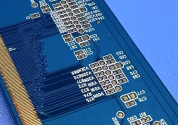
Designing for HDI PCB and Fine-Line Etching: What You Need to Know
As devices shrink and performance demands grow, engineers are turning to High-Density Interconnect (HDI) technology to pack...
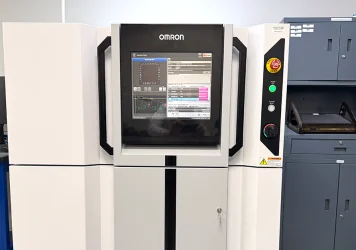
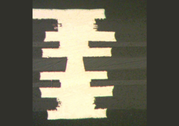
Why AOI and Quality Control Matter in PCB and Flex Circuit Manufacturing
When it comes to PCB and flex circuit manufacturing, even the most well-designed layout can fail if the...
Guide to PCB & FPC Manufacturing Processes
This blog is an excerpt from the white paper Guide to PCB & FPC Manufacturing Processes: Subtractive, Semi-Additive & Additive...
Understanding Solder Masks: Types, Processes, and Usage Guidelines
In PCB manufacturing, solder mask isn’t just about making a board look green—it’s a functional layer that protects copper...
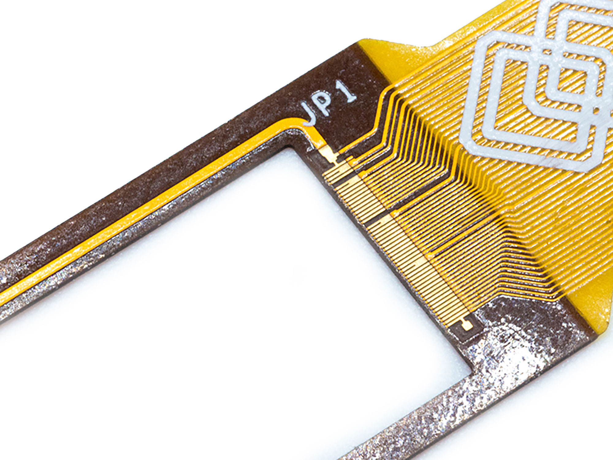
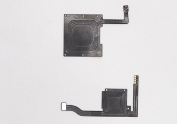
Common Mistakes Made by PCB Designers When Designing Flexible Circuits (FPCs)
Flexible Printed Circuits (FPCs) are widely used due to their lightweight, flexible, and compact nature, making them ideal for...
6-Layer ELIC Rigid Flex Printed Circuit Board / Rigid Flex PCB
A 6-Layer ELIC (Every Layer Inter-connect) Rigid Flex Printed Circuit Board / Rigid Flex PCB is an advanced and...