Understanding Copper Limits & Bend Radius in Flex PCBs
Sebastian Cantu2026-04-21T18:10:41+00:00Whether you’re designing for a high-durability dynamic application or a compact static installation, every detail matters—from copper type and thickness to stackup design and layer placement. These design elements directly influence the PCB’s flexibility, durability, and long-term performance. For electrical and mechanical engineers alike, mastering these principles is key to creating robust and efficient solutions that meet the unique demands of modern applications.
This blog dives into the mechanics of copper in flex and rigid-flex PCBs, providing practical insights to optimize your designs and ensure reliable performance, even under the most demanding conditions.
The Role of Bend Radius in PCB Design
The bend radius is a fundamental design parameter that determines the PCB’s flexibility and durability. Increasing the bend radius reduces stress on the copper conductors in the bend area, enhancing both flexibility and lifespan. Adhering to recommended bend radii prevents conductor strain and failure. Below are general guidelines for various circuit types:
• Single-sided circuits: 3 to 6 times the circuit thickness
• Double-sided circuits: 6 to 10 times the circuit thickness
• Multilayer circuits: 10 to 15 times the circuit thickness
• Dynamic applications: 20 to 40 times the circuit thickness
By optimizing the bend radius, designers can ensure reliability in applications where flexibility is critical, such as medical devices, wearables, and aerospace systems.
For more critical applications where the margin for mechanical failure is minimal—such as in medical devices, aerospace systems, or high-performance robotics—it’s essential to go beyond general guidelines and utilize precise industry standards like IPC-2223 for calculating the minimum bend radius. According to IPC-2223, the bend radius can be calculated by factoring in the material’s modulus of elasticity, copper thickness, and the number of layers in the flex stackup. For example, a double-sided circuit with a thickness of 0.5 mm may require a bend radius closer to 10 mm for static applications and 20 mm or more for dynamic use cases to ensure mechanical integrity. These more rigorous calculations provide engineers with better estimates tailored to the application’s mechanical and operational demands, reducing risks of failure in mission-critical environments.
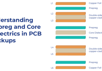
The following examples are based on Southeast Asia (SEA) typical stack-ups, reflecting real-world manufacturing insights from high-volume production. In SEA, designs commonly favor thinner FPC/RF constructions and compact sizes, aligning with trends in mass manufacturing. These are just examples—there are endless possible stack-up combinations, including thicker constructions, depending on specific design and application requirements.
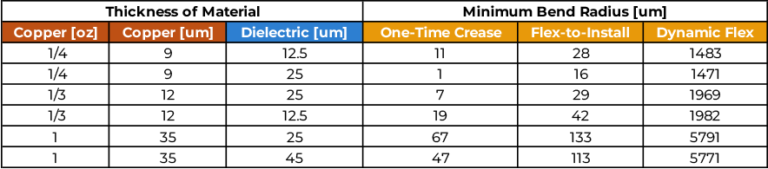
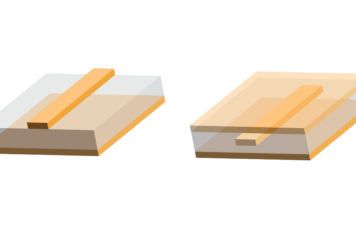
Figure 1: Single-Sided SEA Typical Stackups
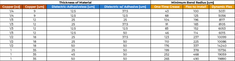
Figure 2: Double-Sided SEA Typical Stackups
Copper Deposition Methods: RA vs. ED Copper
The mechanical performance of copper in flex PCBs is heavily influenced by its deposition method:
1. Rolled Annealed (RA) Copper:
• Known for its superior ductility and fatigue resistance.
• Ideal for high-flex and dynamic applications, where repeated bending is common.
2. Electro-Deposited (ED) Copper:
• Offers excellent electrical conductivity.
• More brittle, making it suitable for static applications with minimal bending.
3. High Ductility Electro-Deposited (HDED) Copper:
• Offers superior flexibility, especially in ultra-thin applications.
• Ideal for extreme bending and highly dynamic designs.
Download our Flexible PCB Materials eBook to learn how substrates, adhesives, conductors, and coverlays impact flex circuit design and long-term performance.
Choosing the right copper type is crucial for matching the PCB’s mechanical demands.
Mechanical Properties of Copper
Copper’s ability to endure mechanical stresses depends on three key properties:
• Tensile Strength: Determines how much force the copper can withstand before breaking
• Ductility: Determines the copper’s ability to deform without breaking or losing integrity.
• Fatigue Resistance: Indicates how well copper endures repeated flex cycles over time.
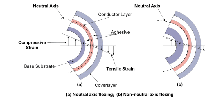
Neutral Axis and Layer Placement
The neutral axis is the point within a PCB where mechanical stress is minimized during bending. Placing copper layers closer to the neutral axis reduces the strain they experience, preventing cracking or deformation. This design consideration is especially important in multilayer PCBs, where layer placement and separation directly impact flexibility and durability.
Stackup Design and Layer Separation
In multilayer flex designs, the stackup influences mechanical performance:
• Layers spaced too far apart increase strain during bending.
• Layers placed too close together reduce overall flexibility.
Optimal layer spacing balances these factors, ensuring the PCB can flex without compromising copper integrity.
Choosing the Right Copper Thickness
The selection of copper thickness involves a trade-off between electrical performance and mechanical flexibility:
• Thicker copper: Offers lower resistance but reduces flexibility.
• Thinner copper: Enhances flexibility but may require design adjustments to meet electrical requirements.
Dynamic vs. Static Applications
The application type significantly influences design priorities:
• Dynamic applications (e.g., robotics, medical devices): Require materials and designs that endure repeated bending without degradation. RA or High-Ductility ED (HDED) copper is ideal.
• Static applications (e.g., installed connectors): Prioritize space and electrical performance over flexibility.
Selecting the appropriate copper type and thickness ensures the PCB meets its intended functionality.
Conclusion
Copper’s mechanical properties, deposition method, and placement within the PCB stackup are critical factors in achieving reliable and flexible designs. By adhering to bend radius guidelines, choosing the right type of copper, and optimizing stackup design, engineers can extend the lifespan and performance of flex and rigid-flex PCBs.
At PICA Manufacturing Solutions, we specialize in designing and manufacturing flex and rigid-flex circuits that meet demanding mechanical and electrical requirements. Contact us to learn more about our expertise and how we can support your next project.