Printed Circuit Boards / PCBs
Custom Printed Circuit Boards Engineered for Performance
PICA designs and manufactures printed circuit boards (PCBs) that deliver precise, reliable performance across industries. From early-stage prototypes to high-volume production, our team provides scalable PCB fabrication backed by stringent quality control and responsive engineering support.
Trusted in medical devices, industrial automation, communications, wearables, and automotive systems, PICA PCBs are built to meet demanding requirements for signal integrity, durability, and manufacturability.
Why Choose Printed Circuit Boards from PICA?
Proven Reliability – Stable boards produced under strict quality standards.
Cost-Effective Options – Single-sided and double-sided PCBs for straightforward applications.
High-Density Interconnects – Multi-layer and HDI designs for compact, high-performance systems.
Design Optimization – Engineering support for stack-ups, materials, impedance, and thermal management.
Scalable Production – Fast prototypes and high-volume builds with global logistics.
PCB Capabilities – Highlights
PICA offers full end-to-end PCB manufacturing with advanced processes and materials:
Up to 28+ layers with complex HDI stack-ups
Microvias, blind & buried vias for compact routing
Controlled impedance with TDR verification
Fine-line circuitry for high-speed and miniaturized designs
Material flexibility – FR-4, high-temp laminates, and hybrid constructions
Thermal management – Optimized for heat dissipation and reliability
Regulatory compliance – RoHS, UL, and ISO 13485 certified manufacturing
For more technical information on PICA’s Printed Circuit Boards capabilities, click the button below.
Benefits of Printed Circuit Boards / PCBs
Consistent Quality
Every board is manufactured under strict process control for long-term reliability.
Design Flexibility
Options from simple single-sided PCBs to advanced multi-layer HDI structures.
Faster Time-to-Market
Quick-turn prototyping and scalable production help you launch products faster.
Optimized Performance
Engineered for signal integrity, thermal stability, and durability in demanding applications.
Global Manufacturing Advantage
U.S. and Malaysia facilities provide cost-effective production with local support.
Markets We Serve with Printed Circuit Boards / PCBs
Consumer Electronics:
Powering compact devices like smartphones, tablets, and wearables with lightweight, space-saving designs.
Medical Devices:
Used in pacemakers, hearing aids, implants, and diagnostics where flexibility and reliability are critical.
Automotive:
Built into control modules, lighting, and infotainment systems to withstand vibration, heat, and irregular layouts.
Industrial Equipment:
Trusted in robotics, sensors, and control systems for durability in harsh environments.
Defense & Security:
Essential in satellites, missiles, and avionics, combining lightweight efficiency with extreme durability.

PCB, Flex & PCBA Cost Pressures in 2026: What OEMs Need to Watch
Electronics manufacturing is heading into 2026 under pressure from several directions at once. Rising metals costs, laminate and prepreg repricing,...

CES 2026 Highlights: The Breakthrough Technologies Powered by Advanced Flex & PCB Design
Las Vegas, January 2026 — CES 2026 once again confirmed that the pace of innovation in consumer tech, mobility,...

Designing PCBs for Medical Devices: Key Considerations & Compliance Tips
PCB design for medical electronics demands more than just electrical functionality. Devices must meet...
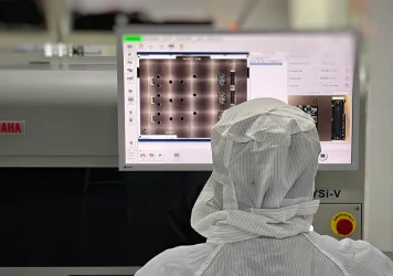
See What You Can’t See: AOI & X‑Ray Inspection in PCB Assembly
In today’s electronics world, component densities are rising, geometries are shrinking, and reliability expectations are higher than ever. Failures at...
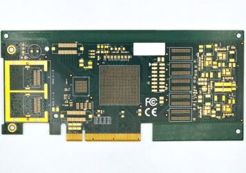
Designing for Edge-Mounted PCBs: Best Practices and Considerations
When space is tight, or when PCBs need to mate with enclosures, panels, or external interfaces, edge-mounted boards can offer...
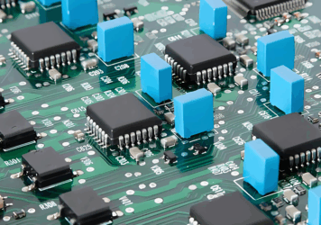
Mastering Thermal Management in PCB and Flex Circuit Design
As electronic devices become more compact and powerful, managing heat effectively is critical to ensuring performance, reliability, and long product...
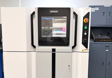
Why AOI and Quality Control Matter in PCB and Flex Circuit Manufacturing
When it comes to PCB and flex circuit manufacturing, even the most well-designed layout can fail if the...
Guide to PCB & FPC Manufacturing Processes
This blog is an excerpt from the white paper Guide to PCB & FPC Manufacturing Processes: Subtractive, Semi-Additive & Additive...
Request Your PICAKit Today
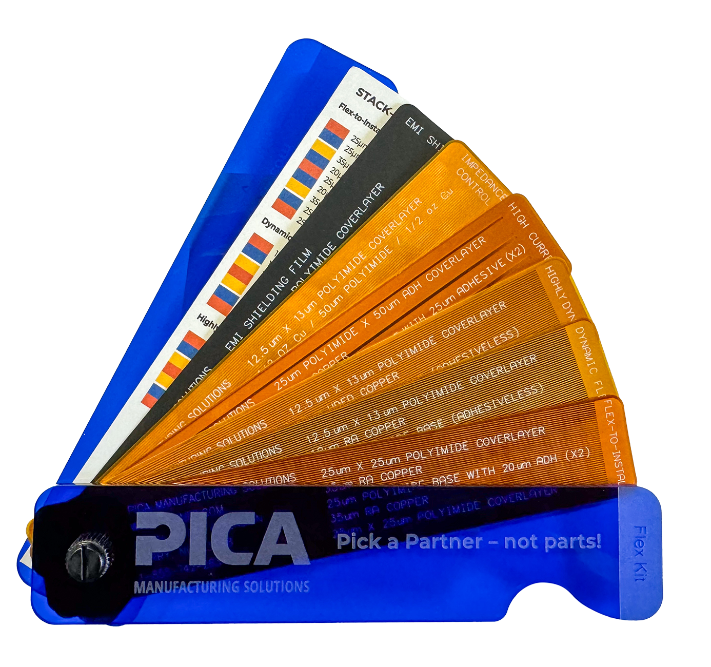
We want you to take a look at what we can produce for you by offering you a PICAKit which includes a variety of flexible pcb, shields, & flat flexible cables.
