Controlled Impedance in Printed Circuit Board Design
FlexPros2026-04-02T13:04:08+00:00In the design of printed circuit boards (PCBs), controlling impedance is a crucial factor for ensuring optimal signal integrity, especially in high-frequency applications. Impedance mismatches can lead to signal reflections, data loss, and compromised performance, which makes it essential to consider various transmission line configurations and impedance types during the design process. This paper explores the fundamentals of controlled impedance, focusing on key factors such as dielectric materials, copper thickness, trace width, and spacing. By understanding these principles, PCB designers can ensure proper signal transmission and minimize interference, ultimately achieving reliable and efficient PCB functionality.
Signal Transmission Lines
Signal transmission lines in circuit systems are composed of conductors (signal lines), an insulating dielectric layer, and a ground layer (large copper surface). These components collectively propagate high-frequency signals or electromagnetic waves. The configurations include:
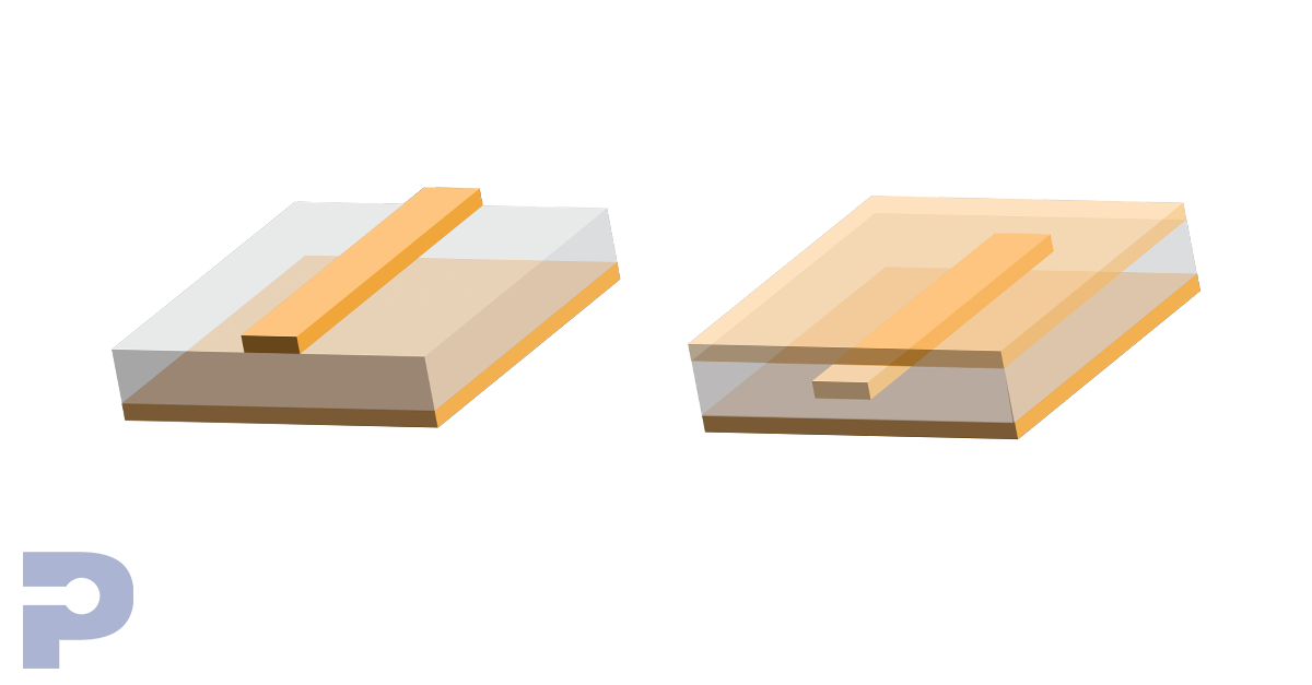
Microstrip: An external PCB trace adjacent to a solid plane via a dielectric material. It suppresses RF on the PCB and allows faster clock and logic signals compared to stripline due to lower coupling capacitance and propagation delay. However, without metallic shielding above and below, this layer can radiate RF energy into the environment.

Surface Microstrip
Embedded Microstrip: Here, the signal trace is embedded within the dielectric material rather than on the surface, reducing electromagnetic radiation and enhancing signal integrity. This setup is suited for high-speed digital circuits needing controlled impedance and reduced cross-talk.
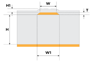
Coated Microstrip
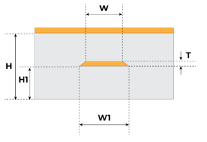
Embedded Microstrip
Stripline (Inner Layer Signal Line): Positioned between two solid planes (Voltage or Ground), it provides excellent radiation shielding but is suitable for lower transmission speeds due to capacitive coupling, which reduces the edge rate of high-speed signals.
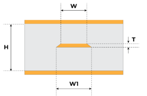
Symmetrical Stripline
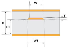
Offset Stripline
Differential Stripline (Inner Layer Signal Line): Consists of two parallel signal traces sandwiched between two ground planes, ensuring isolation from external interference and minimizing electromagnetic radiation, ideal for high-frequency transmission environments.
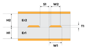
Differential Stripline
Impedance Types
Characteristic Impedance: The impedance between two conductors when insulated from the ground, typically below 80Ω for a single line. Impedance values can vary slightly before and after solder resist application.
Differential Impedance: Measured between two conductors, usually above 80Ω for high-frequency pairs, considering the spacing for impedance calculation.
Controlled impedance is critical to signal integrity, high-speed performance, and long-term PCB reliability. Explore PICA’s impedance control capabilities for solutions built around demanding electrical and design requirements.
Factors Affecting Impedance & Production Process Monitoring
Dielectric Constant (Dk): Mostly determined by the raw materials, with variations in Dk affecting the characteristic impedance significantly.
Copper Thickness (T): Influenced by raw materials and manufacturing capabilities, copper thickness is crucial for maintaining desired impedance levels.
Trace Width (W): Critical for achieving specific impedance values, controlled through precise manufacturing processes.
Interlayer Insulation Thickness (H): A key factor in impedance control, dependent on the core and prepreg thickness as well as the copper retention rate in the design.
Trace Spacing: Plays a significant role in differential impedance, requiring accurate monitoring during production.
Impedance Testing: During PCB production, impedance values are measured and compared with design values using a Time Domain Reflectometer (TDR). This device checks the characteristic impedance by emitting a “voltage”-type “step wave” along a transmission cable, identifying any impedance discrepancies due to signal line defects.
The image illustrates how, in an ideal scenario, signals and voltage layers are clean and consistent, while in a real-world scenario, noise and fluctuations can be present on both the signal and the power/ground layers.
Controlled impedance is essential for maintaining signal integrity in high-frequency PCB designs. By carefully managing factors like dielectric constant, copper thickness, trace width, and spacing, designers can reduce signal interference and ensure reliable performance. As technology advances, precise impedance control will remain critical for high-speed applications

