Minimizing Material Waste Through Optimized Nesting
Janet Shi2025-07-23T17:55:44+00:00When designing flexible circuits, especially those with irregular shapes, it’s easy to overlook how layout decisions impact manufacturing efficiency. But how your parts are nested within a panel directly affects both material waste and cost. That’s why it’s important to consider panel optimization early in the design process—not just during fabrication.
At PICA Manufacturing Solutions, we work closely with customers to improve yield and reduce waste through smart panelization and nesting strategies. Here’s how a few small decisions in the design phase can lead to big savings later.
Why Nesting Matters
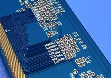
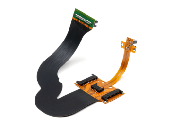
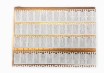
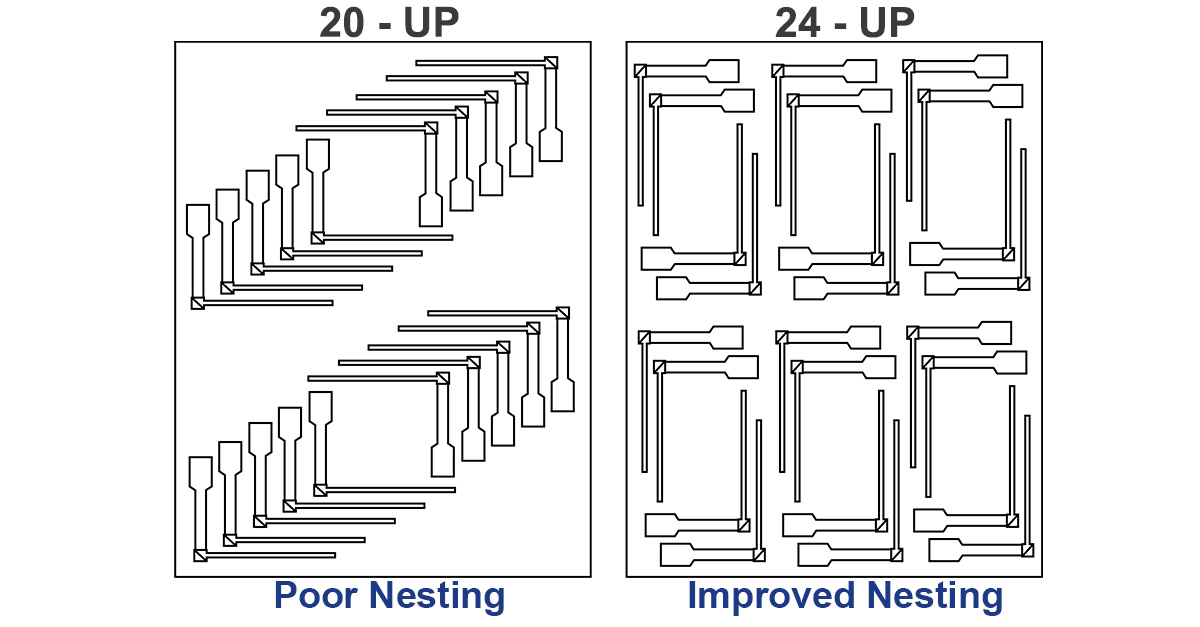
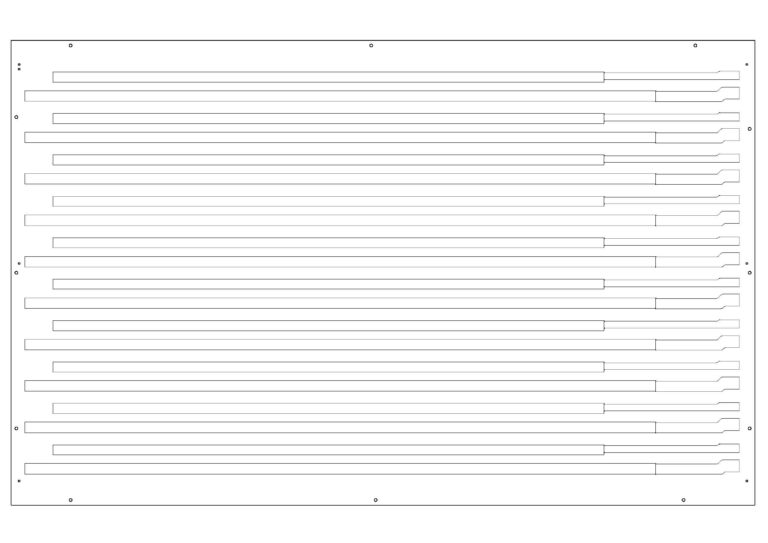
In flex circuit manufacturing, “nesting” refers to how individual circuit shapes are arranged within a standard sheet or panel of raw material. Because many flex designs are non-rectangular, poor nesting can lead to unused or unusable areas of the panel—driving up material costs.
For high-volume production or circuits made with premium materials (like rolled annealed copper or polyimide), optimizing the layout can make a major difference in total cost per unit.
Design Tips for Better Nesting and Less Waste
- Consider Grain Direction of Copper
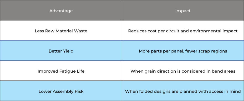
For dynamic flex applications—especially those with repeated bending—it’s important that conductors in the bend region run parallel to the grain direction of the rolled annealed (RA) copper foil. While this limits nesting options slightly, it significantly improves fatigue resistance and long-term reliability.
If you’re unsure about the copper grain direction on a specific design or material, we can help advise before layout is finalized.
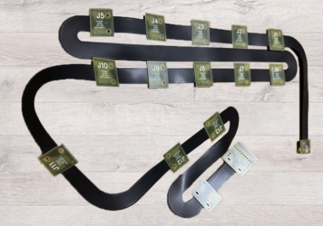
- Plan for Folded Designs Carefully
In some cases, folds are used within the design to further optimize how circuits fit within the panel. While this can reduce space, it also changes the orientation of pads and access points after folding.
Ensure that access areas are still reachable and properly aligned once the circuit is assembled and folded—especially for testing, connector placement, or component soldering.
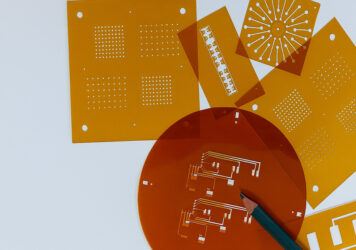
- Avoid Non-Nesting Shapes Where Possible
Try to maintain edge alignments or symmetry in your outline when you can. Designs with heavy asymmetry, extreme tapers, or unbalanced wings can leave large negative spaces on the panel that can’t be reused.
If your functional shape is inherently irregular, we can help explore whether slight outline adjustments could improve material utilization without compromising functionality.
Discover how the right materials—from substrates to laminates—impact performance, durability, and cost. Dive into our blog series and make smarter design decisions today.
- Ask About Shared Tooling
In some cases, multiple part numbers with compatible dimensions can be combined onto a single panel to improve yield. If you’re producing similar variants or left/right versions of the same part, let us know early—we may be able to combine them to reduce overall waste.
Benefits of Optimized Nesting
Work With Us Early
The best time to talk about nesting and material optimization is before your layout is finalized. Our engineering team can review your design outline, material selection, and intended usage to help you:
• Improve material utilization
• Align copper direction for better mechanical life
• Avoid costly post-layout revisions
At PICA Manufacturing Solutions, we’re more than just a fabricator—we’re your design partner. Reach out to us early in your process, and let’s make your flex circuit not only functional, but optimized for performance, yield, and sustainability.