

PCB, Flex & PCBA Cost Pressures in 2026: What OEMs Need to Watch
Electronics manufacturing is heading into 2026 under pressure from several directions at once. Rising metals costs, laminate and prepreg repricing,...

CES 2026 Highlights: The Breakthrough Technologies Powered by Advanced Flex & PCB Design
Las Vegas, January 2026 — CES 2026 once again confirmed that the pace of innovation in consumer tech, mobility,...

Designing PCBs for Medical Devices: Key Considerations & Compliance Tips
PCB design for medical electronics demands more than just electrical functionality. Devices must meet...
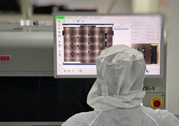
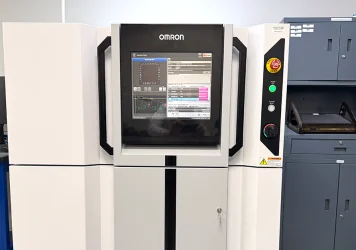
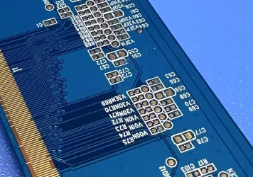
See What You Can’t See: AOI & X‑Ray Inspection in PCB Assembly
In today’s electronics world, component densities are rising, geometries are shrinking, and reliability expectations are higher than ever. Failures at...
Designing for Edge-Mounted PCBs: Best Practices and Considerations
When space is tight, or when PCBs need to mate with enclosures, panels, or external interfaces, edge-mounted boards can offer...
Mastering Thermal Management in PCB and Flex Circuit Design
As electronic devices become more compact and powerful, managing heat effectively is critical to ensuring performance, reliability, and long product...
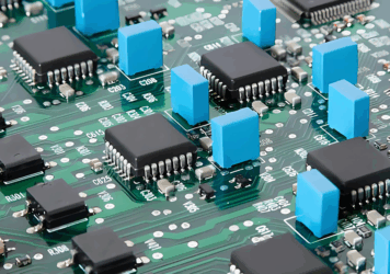
Why AOI and Quality Control Matter in PCB and Flex Circuit Manufacturing
When it comes to PCB and flex circuit manufacturing, even the most well-designed layout can fail if the...
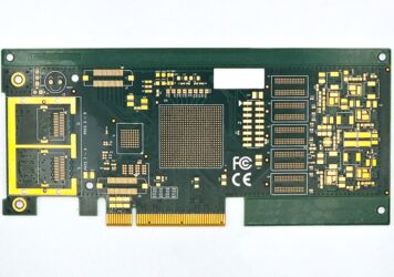
Guide to PCB & FPC Manufacturing Processes
This blog is an excerpt from the white paper Guide to PCB & FPC Manufacturing Processes: Subtractive, Semi-Additive & Additive...